SP (Surface Plasmon) wave signal amplifier and manufacturing method thereof

A surface plasmon wave and signal amplifier technology, applied in the field of ion waves, can solve the problem of short propagation length of SP waves and achieve the effect of increasing the propagation length

Inactive Publication Date: 2013-12-18
YANSHAN UNIV
View PDF5 Cites 0 Cited by
  • Summary
  • Abstract
  • Description
  • Claims
  • Application Information

AI Technical Summary

Problems solved by technology

[0004] The problem to be solved by the present invention is to provide a surface plasmon wave signal amplifier and its manufacturing method, to overcome the shortcoming of SP wave propagation length in the prior art

Method used


Image

  • SP (Surface Plasmon) wave signal amplifier and manufacturing method thereof
  • SP (Surface Plasmon) wave signal amplifier and manufacturing method thereof
  • SP (Surface Plasmon) wave signal amplifier and manufacturing method thereof

Examples


Embodiment 1

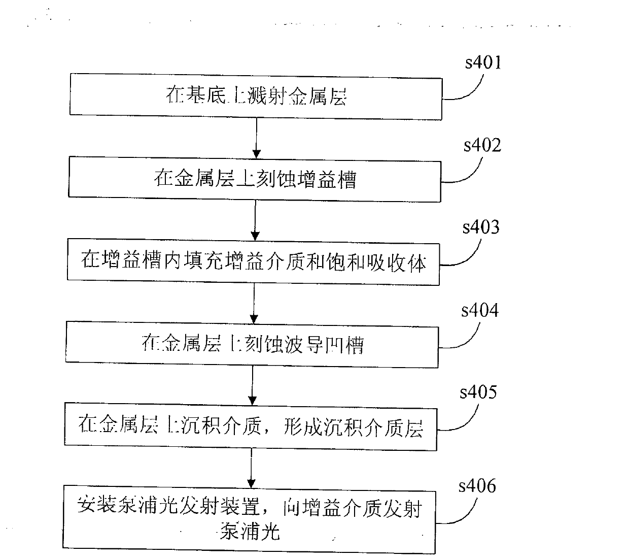
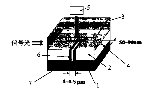
[0035] The structure of a surface plasmon wave signal amplifier in this embodiment is as follows figure 1 As shown, including substrate 1, metal layer 2 and deposition medium layer 3;

[0036] The metal layer 2 is located between the substrate 1 and the deposition medium layer 3, its top surface is connected to the bottom surface of the deposition medium layer 3, and the bottom surface is connected to the top surface of the substrate 1;

[0037] The top surface of the metal layer 2 is provided with a waveguide groove penetrating both sides, and the width of the waveguide groove is 50-90nm; the bottom surface of the deposition medium layer 3 is provided with a protrusion corresponding to the waveguide groove , the waveguide grooves and protrusions form a MIM (metal-medium-metal) waveguide 4, and signal light is transmitted through the waveguide 4;

[0038] A gain slot is formed on the side wall of the waveguide 4, the width of the gain slot is 1-1.5 μm, and the gain slot is fi...

Embodiment 2

[0044] The structure of a surface plasmon wave signal amplifier in this embodiment is as follows figure 2 As shown, its basic structure is the same as that of Embodiment 1. The difference between this embodiment and Embodiment 1 is that a branch structure 8 is provided on the other side wall of the waveguide 4, and the branch structure 8 is connected to the gain Opposite to the groove, the branch structure 8 is used to increase the Q value of the equivalent SP cavity.

Embodiment 3

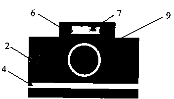
[0046] The structure of a surface plasmon wave signal amplifier in this embodiment is as follows image 3 As shown, its basic structure is the same as that of Embodiment 1. The difference between this embodiment and Embodiment 1 is that a resonant ring coupling structure 9 is provided on the top surface of the metal layer 2, and the resonant ring coupling structure 9 is a ring structure. , the plasma wave of a specific wavelength determined by its size can be coupled through the resonant ring coupling structure 9. In this embodiment, the resonant ring coupling structure 9 is an annular metal cavity as shown in the figure, which is located between the waveguide and the gain medium to realize The coupling effect of the two. The surface plasmon wave signal amplifier of this embodiment is mainly used in occasions that require a higher signal wave mode.


PUM


Abstract

The invention discloses an SP (Surface Plasmon) wave signal amplifier, which comprises a substrate, a metal layer and a deposited dielectric layer. The metal layer is located between the substrate and the deposited dielectric layer, the top face of the metal layer is connected with the bottom face of the deposited dielectric layer, and the bottom face of the metal layer is connected with the top face of the substrate; a waveguide penetrating the two sides of the top face of the metal layer is arranged at the top face of the metal layer; a gain slot is formed in the sidewall of the waveguide, the width of the gain slot is 1-1.5 microns, and a gain medium and a saturable absorber are filled in the gain slot; and the amplifier further comprises a pump light emitting device which is used for emitting pump light exciting the gain medium. The invention further discloses a manufacturing method of the SP wave signal amplifier. According to the SP wave signal amplifier, the ultra-fast signal amplification of SP waves transmitted by the SP waveguide can be realized, so that the propagation length of the SP waves is increased.

Description

technical field [0001] The invention relates to the technical field of surface plasmon waves, in particular to a surface plasmon wave signal amplifier and a manufacturing method thereof. Background technique [0002] SP (Surface Plasmon, surface plasmon) wave is a kind of non-radiative electromagnetic wave propagating on the surface of metal and medium, and it is an important research field of nanophotonics. Using the properties of SP waves, sub-wavelength photonic devices can be realized, breaking through the limitations of traditional integrated optoelectronic technology, and have broad application prospects in future high-speed communication systems, integrated photonic information processing systems, and new biophotonic sensors. [0003] However, due to the ohmic effect in metals, there is a strong loss in SP wave transmission. Even if the long-range SPP (Surface Plasmon Polariton, surface plasmon polariton) waveguide technology is used, the propagation length in the vis...

Claims


Application Information

Patent Timeline
Patent Type & Authority Patents(China)
IPC IPC(8): H01S4/00
Inventor 李志全牛力勇孙宇超李欣李文超沙晓鹏
Owner YANSHAN UNIV
Why Eureka
Try Eureka