Micro-grating optical cavity structure and manufacturing method for enhancing near-infrared response of silicon detector

A manufacturing method and detector technology, applied in the direction of microstructure technology, microstructure devices, manufacturing microstructure devices, etc., can solve the problems of detector near-infrared response decline, device performance degradation, and high equipment requirements, and achieve process compatibility and ease of use. Integrate and improve the effect of response

Active Publication Date: 2020-08-18
THE 44TH INST OF CHINA ELECTRONICS TECH GROUP CORP
View PDF9 Cites 0 Cited by
  • Summary
  • Abstract
  • Description
  • Claims
  • Application Information

AI Technical Summary

Problems solved by technology

However, using a femtosecond laser to make supersaturated sulfur-doped black silicon on the back of the detector involves depositing an aluminum oxide passivation layer on the surface of the black silicon by atomic layer deposition, which is complex and requires high equipment requirements. During the high-temperature annealing process in the process of making the detector, sulfur ions will be precipitated, the near-infrared response of the detector will be greatly reduced, and the performance of the device will be seriously degraded.

Method used


Image

  • Micro-grating optical cavity structure and manufacturing method for enhancing near-infrared response of silicon detector
  • Micro-grating optical cavity structure and manufacturing method for enhancing near-infrared response of silicon detector
  • Micro-grating optical cavity structure and manufacturing method for enhancing near-infrared response of silicon detector

Examples


Embodiment 1

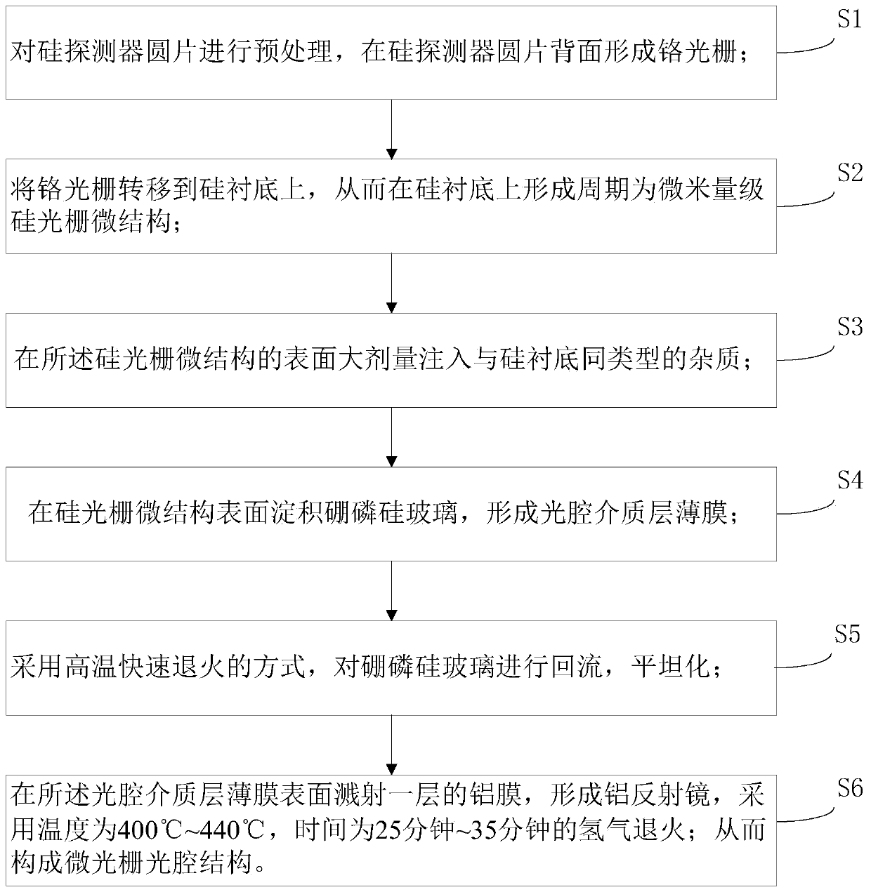
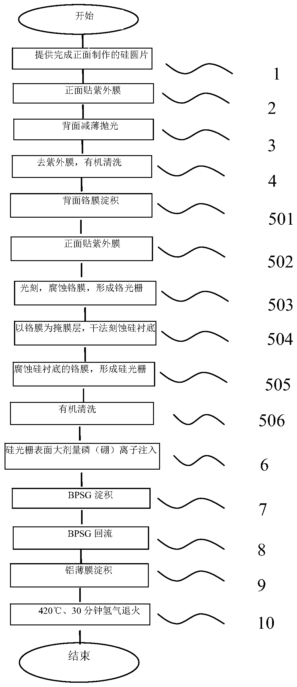
[0035] A method for manufacturing a micro-grating optical cavity structure that enhances the near-infrared response of a silicon detector adopted in the present invention, such as figure 1 Shown include:

[0036] S1. Pre-treat the silicon detector wafer, paste ultraviolet film on the front of the silicon detector wafer to protect the front structure of the detector; thin and polish the back of the silicon detector wafer to the required thickness; remove the detection Use acetone and ethanol to organically clean the UV film on the front of the device disc. Form a chromium grating on the back of the detector; deposit a 20nm chromium film on the back of the detector wafer; paste a UV film on the front of the detector wafer, apply glue on the back, and photolithography, and transfer the periodically arranged grating pattern to the chromium film; Use chromium etching solution to etch the chromium film not protected by photoresist, organically remove the glue, and form a chromium g...

Embodiment 2

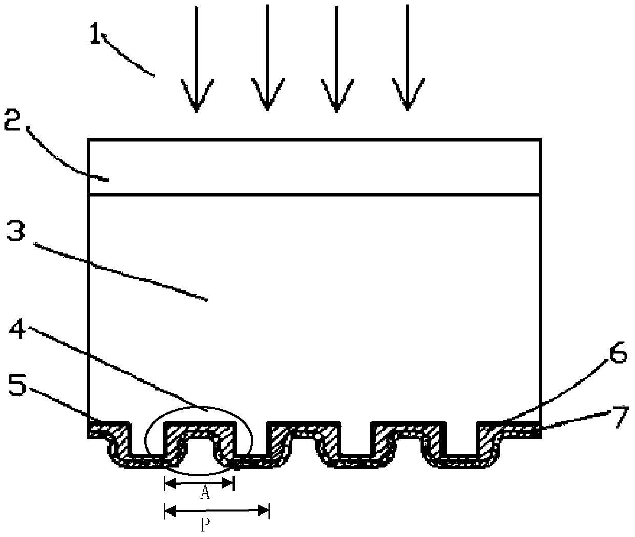
[0048] combine figure 2 and image 3 , to further illustrate the silicon grating micro-optical cavity structure of the present invention;

[0049] Light 1 is incident from the front of the detector and enters the silicon detector wafer 2 (including detector electrodes, guard rings, cut-offs, PN junctions, anti-reflection coatings and other structures, and the present invention does not relate to the production of silicon detector wafers 2) The silicon substrate 3 is made of silicon material to absorb the incident light 1; the impurity 5 is injected into the microstructure of the silicon grating in large doses, and then the borophosphosilicate glass medium is reflowed and planarized to form a BPSG optical cavity dielectric layer 6, which is placed in the optical cavity A layer of aluminum film is sputtered on the surface of the thin film of the dielectric layer 6 to form an aluminum mirror 7 . thus constitute as figure 2 The micro-grating optical cavity 4 shown;

[0050] ...


PUM

PropertyMeasurementUnit
quantum efficiencyaaaaaaaaaa

Abstract

The invention belongs to the field of photoelectric technology, in particular to a micro-grating optical cavity structure for enhancing near-infrared response of a silicon detector and a manufacturingmethod thereof. The fabrication process of the micro-grating optical cavity is integrated into the fabrication process of silicon detector, which is compatible with the fabrication process of the micro-grating optical cavity. The method comprises: pretreating a silicon detector wafer to form a chromium grating on the back surface of the detector wafer; transferring the chromium grating onto a silicon substrate to form a silicon grate microstructure with a period of micron on that silicon substrate; implanting the high dose of impurities of the same type as silicon substrate on the surface ofsilicon grating microstructure,and depositing boron phosphor silicon glass on the surface to form an optical cavity dielectric layer film; refluxing and planarizing boron phosphate silicate glass by high temperature and rapid annealing, sputterring a lay of aluminum film on the surface of the thin film of the optical cavity dielectric lay to form an aluminum mirror; and forming a light cavity structure of that micro grate. The invention relates to a backreflection structure of a silicon detector, which binds incident photons in the silicon detector, thus prolonging its propagation path, and remarkably improving the absorption efficiency of the silicon detector.

Description

technical field [0001] The invention belongs to the field of optoelectronic technology, in particular to a micro-grating optical cavity structure and a manufacturing method for enhancing the near-infrared response of a silicon detector. Background technique [0002] Silicon has a high absorption coefficient in ultraviolet and visible light, but a low absorption coefficient in the near-infrared band. For light with a wavelength of 1064nm, the absorption length of silicon is greater than 250 μm. In order to increase the near-infrared response of the silicon detector, the absorption thickness of the silicon substrate needs to be increased. With the increase of the thickness of the silicon substrate, the drift time of photogenerated carriers increases and the response speed decreases. Applying a higher reverse bias voltage to fully deplete the silicon substrate will increase the response speed, but will generate greater dark current and noise. In order to improve the sensitivit...

Claims


Application Information

Patent Timeline
Patent Type & Authority Patents(China)
IPC IPC(8): B81C1/00B81B7/02
CPCB81B7/02B81B2201/04B81C1/00015
Inventor 李华高郭培
Owner THE 44TH INST OF CHINA ELECTRONICS TECH GROUP CORP
Why Eureka
Try Eureka