Organic photosensitive optoelectronic devices
A photoelectric device and device technology, applied in the field of organic photosensitive optoelectronic devices, can solve the problems of increased light absorption and inability to harvest incident light
- Summary
- Abstract
- Description
- Claims
- Application Information
AI Technical Summary
Problems solved by technology
Method used
Image

Examples
Embodiment Construction
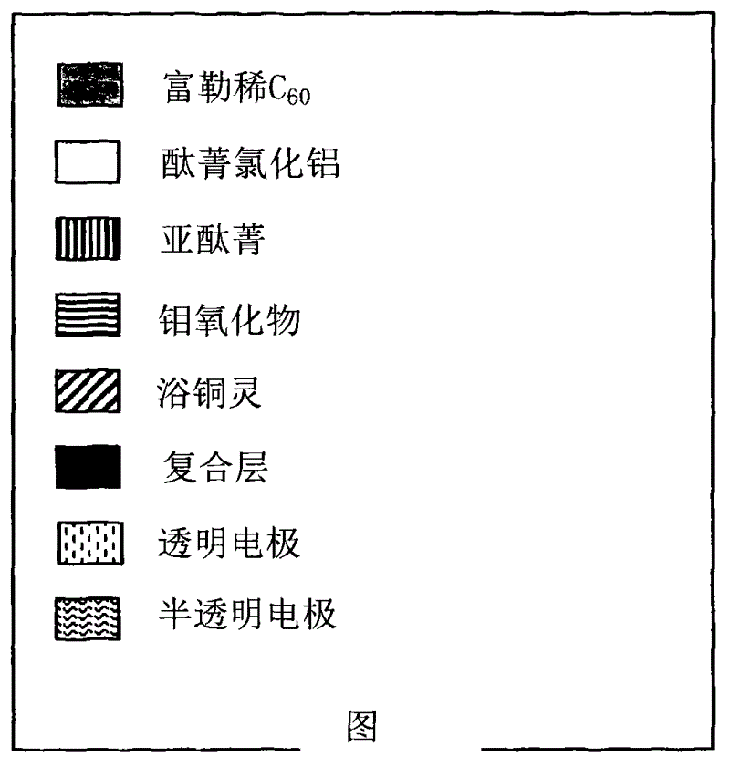
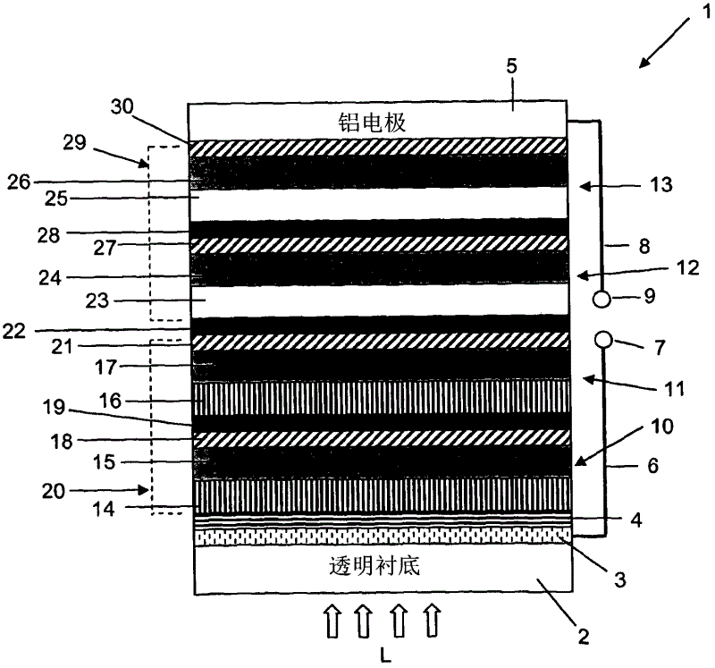
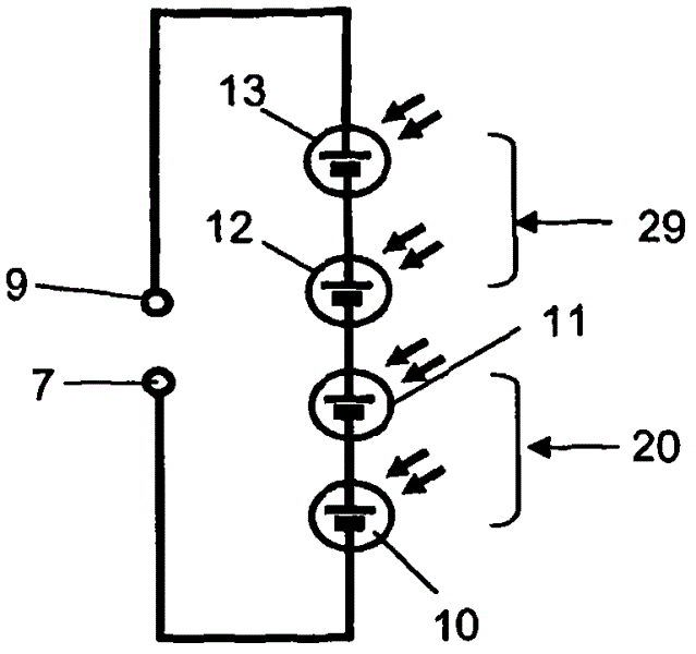
[0036] figure 1 show as figure 2 , 4 and 5 show layer legends. Fullerene C 60 Used as a receptor layer. Chloro-aluminium phthalocyanine and subphthalocyanine were used as the donor layer. Molybdenum oxide serves as an interlayer between the anode and the donor layer of the subcell. Bathocuproine (BCP) was used as an exciton blocking layer. The composite layer can be formed in the form of a thin translucent metal layer of silver, aluminum or titanium, or it can be a metal such as indium tin oxide (ITO), zinc indium tin oxide or gallium indium tin oxide. ) and other transparent layers of conductive oxides, or can provide discontinuous recombination centers. The transparent electrode may be a transparent layer of a conductive oxide, such as indium tin oxide (ITO), indium tin zinc oxide or indium tin gallium oxide. The translucent electrodes can be thin metallic layers of silver, aluminum or titanium.
[0037] figure 1 An organic semiconductor photovoltaic device 1 accor...
PUM
 Abstract
Description
Claims
Application Information