Light emitting diode (LED) chip structure

A technology of light-emitting diode and chip structure, applied in electrical components, circuits, semiconductor devices, etc., can solve the problems of large difference in refractive index and inability to export chips, etc., to improve the injection efficiency, reduce the operating voltage of the device, and improve the current expansion. Effect

Inactive Publication Date: 2012-08-15
EPILIGHT TECH
View PDF3 Cites 10 Cited by
  • Summary
  • Abstract
  • Description
  • Claims
  • Application Information

AI Technical Summary

Problems solved by technology

The light extraction efficiency of the chip is the main factor limiting the external quantum efficiency of the device. The main reason is that the refractive index difference between the epitaxial material, th

Method used


Image

  • Light emitting diode (LED) chip structure
  • Light emitting diode (LED) chip structure
  • Light emitting diode (LED) chip structure

Examples


Embodiment Construction

[0025] Preferred embodiments of the present invention will be further described below in conjunction with the accompanying drawings, which are not drawn to scale for the convenience of illustration.

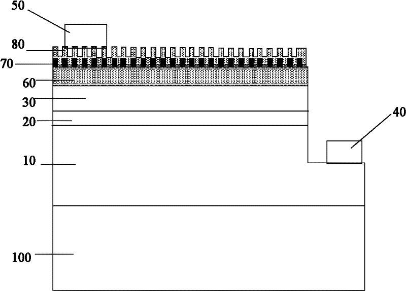
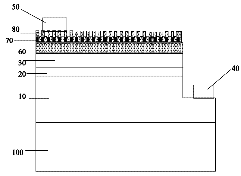
[0026] Please see figure 1 The light emitting diode chip provided in this embodiment includes: an N-type semiconductor layer 10, an active layer 20 located on the N-type semiconductor layer 10, a P-type semiconductor layer 30 located on the active layer 20, and The N electrode 40 electrically connected to the N-type semiconductor layer 10 and the P electrode 50 electrically connected to the P-type semiconductor layer 30; wherein, the N-type semiconductor layer 10 is preferably an N-type GaN layer, and the P-type semiconductor layer 30 It is preferably a P-type GaN layer, and the active layer 20 is preferably a GaN-based quantum well layer. The material layer of the light-emitting diode chip is prepared on the growth substrate 100, the growth substrate 100 is a Si substrate, a sa...


PUM

PropertyMeasurementUnit
Thicknessaaaaaaaaaa
Thicknessaaaaaaaaaa
Diameteraaaaaaaaaa

Abstract

The invention discloses a light emitting diode (LED) chip structure. A P type ohm contact electrode layer is arranged on a P type semiconductor layer of the structure, an insulation blocking structure is arranged on the P type ohm contact electrode layer, a P type transparent conducting layer is arranged on the insulation blocking structure, the insulation blocking structure is covered by the P type transparent conducting layer, and the P electrode is in contact with the P type transparent conducting layer, wherein the insulation blocking structure comprises a plurality of cylindrical insulation structure or is a insulation layer provided with a plurality of through holes. The LED chip structure provided by the invention has the advantages that the current injection efficiency is improved through improving the current expansion, so the LED brightness is improved.

Description

technical field [0001] The invention relates to a light emitting diode structure, in particular to a light emitting diode chip structure with a special electrode structure. Background technique [0002] Light-emitting diodes (LEDs) have the advantages of small size, high efficiency and long life, and are widely used in traffic indication, outdoor full-color display and other fields. In particular, the use of high-power light-emitting diodes may realize semiconductor solid-state lighting, which has caused a revolution in the history of human lighting, and has gradually become a research hotspot in the field of electronics. [0003] In order to obtain high-brightness light-emitting diodes, the key is to improve the internal quantum efficiency and external quantum efficiency of the device. The light extraction efficiency of the chip is the main factor limiting the external quantum efficiency of the device. The main reason is that the refractive index difference between the epi...

Claims


Application Information

Patent Timeline
IPC IPC(8): H01L33/36H01L33/38
Inventor 张楠齐胜利潘尧波郝茂盛
Owner EPILIGHT TECH
Why Eureka
Try Eureka