Electroluminescence device

A technology of electroluminescent devices and light-emitting layers, which is applied in the direction of electric solid-state devices, electrical components, semiconductor devices, etc., can solve the problems of reducing device life, increasing device temperature, and restricting blue light emission, so as to improve energy utilization and luminescence Efficiency enhancement, the effect of improving luminous efficiency

Active Publication Date: 2012-08-29
OCEANS KING LIGHTING SCI&TECH CO LTD +1
View PDF4 Cites 18 Cited by
  • Summary
  • Abstract
  • Description
  • Claims
  • Application Information

AI Technical Summary

Problems solved by technology

[0004] Luminescent materials are the most important factor affecting luminous efficiency. Luminescent materials can be divided into fluorescent materials and phosphorescent materials. Fluorescent materials are blocked by triplet transitions, so they can only emit light through radiation inactivation of singlet states. Triplet excitons and The ratio of singlet excitons is about 3:1; since only 25% of the excitons in the fluorescent material can be effectively used, the remaining 75% are attenuated by non-radiation, and the energy is released in the form of heat, which increases the temperature

Method used


Image

  • Electroluminescence device
  • Electroluminescence device
  • Electroluminescence device

Examples


Embodiment 1

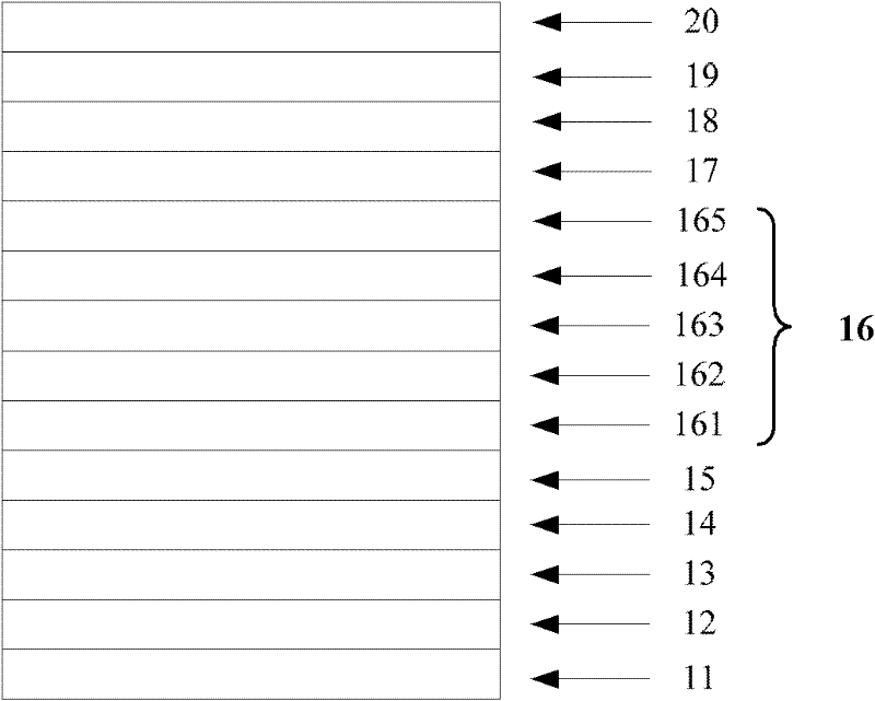
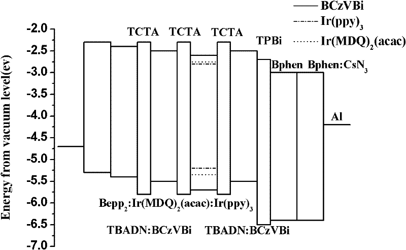
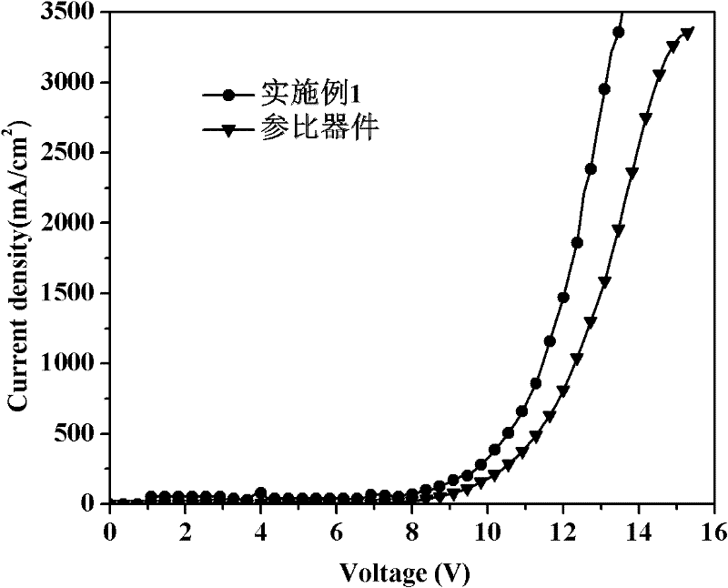
[0035] An electroluminescent device, its structure is: glass / ITO / MoO 3 / NPB / TCTA / TBADN:BCzVBi / TCTA / Bepp 2 :Ir(MDQ) 2 (acac):Ir(ppy) 3 / TCTA / TBADN:BCzVBi / TPBi / Bphen / Bphen:CsN 3 / Al.

[0036] Regarding the electroluminescent device in this example, according to its structure, and using evaporation technology, each organic functional layer is prepared by evaporation in turn; wherein, in the composite structure of the light-emitting layer: the blue light of the first and second blue light-emitting layers The material is BCzVBi, the host material, that is, the hole transport material is TBADN, the doping ratio of the blue light material is 10%, and the thickness is 10nm; the first quantum well material is TCTA, and the thickness is 2nm; in the red-green phosphorescent emitting layer, The red light material is Ir(MDQ) 2 (acac), the doping ratio of the red light material is 1%, and the green light material is Ir(ppy) 3 , the doping ratio of the green light material is 7%, the t...

Embodiment 2

[0044] An electroluminescent device, its structure is: glass / ITO / WO 3 / TPD / TCTA / TPD:BCzVB / TPD / BeBq 2 :Ir(MDQ) 2 (acac):Ir(ppy) 3 / TPD / TPD:BCzVB / TAZ / TPBI / Cs 2 CO 3 / Al.

[0045] Regarding the electroluminescent device in this example, according to its structure, and using evaporation technology, each organic functional layer is prepared by evaporation in turn; wherein, in the composite structure of the light-emitting layer: the blue light of the first and second blue light-emitting layers The material is BCzVB, the host material, that is, the hole transport material is TPD, the doping ratio of the blue light material is 5%, and the thickness is 10nm; the first quantum well material is TPD, and the thickness is 2nm; in the red-green phosphorescence emitting layer, The red light material is Ir(MDQ) 2 (acac), the doping ratio of the red light material is 0.5%, and the green light material is Ir(ppy) 3 , the doping ratio of the green light material is 7%, the thickness of th...

Embodiment 3

[0047] An electroluminescent device, its structure is: glass / ITO / VO x / TDAPB / NPB / TCTA:TBPe / NPB / BeMQ 2 :Ir(MDQ) 2 (acac):Ir(ppy) 3 / TDAPB / TCTA:TBPe / BND / TPQ / LiF / Al.

[0048] Regarding the electroluminescent device in this example, according to its structure, and using evaporation technology, each organic functional layer is prepared by evaporation in turn; wherein, in the composite structure of the light-emitting layer: the blue light of the first and second blue light-emitting layers The material is TBPe, the host material, that is, the hole transport material is TCTA, the doping ratio of the blue light material is 20%, and the thickness is 10nm; the first quantum well material is NPB, and the thickness is 2nm; in the red-green phosphorescence emitting layer, The red light material is Ir(MDQ) 2 (acac), the doping ratio of the red light material is 5%, and the green light material is Ir(ppy) 3 , the doping ratio of the green light material is 10%, the thickness of the red...


PUM

PropertyMeasurementUnit
Thicknessaaaaaaaaaa
Thicknessaaaaaaaaaa
Thicknessaaaaaaaaaa

Abstract

The invention discloses an electroluminescence device, which structurally and sequentially includes a substrate/a conducting layer/a hole injection layer/a hole transmission layer/an electronic blocking layer/a luminous layer/a hole blocking layer/an electronic transmission layer/an electronic injection layer/a cathode layer, wherein the luminous layer adopts a composite layer structure; the composite layer structure sequentially includes a first blue light luminous layer/a first quantum well/a red light-green light phosphorescence luminous layer/a second quantum well/a second blue light luminous layer; the first blue light luminous layer is prepared on the surface of the electronic blocking layer; and the hole blocking layer is prepared on the surface of the second blue light luminous layer. According to the electroluminescence device provided by the invention, the first and the second blue light luminous layers are placed on the two sides of the red light-green light phosphorescence luminous layer respectively, so that the illumination of the red light and the green light can be completely excited by the emitted blue light, the energy utilization ratio is improved, and further the luminous efficiency can be enhanced.

Description

technical field [0001] The invention relates to an electroluminescence device. Background technique [0002] In 1987, C.W.Tang and Van Slyke of Eastman Kodak Company in the United States reported a breakthrough in the research of organic electroluminescence. A high-brightness, high-efficiency double-layer organic electroluminescent device (OLED) was prepared by using ultra-thin film technology. In this double-layer structure device, the brightness reaches 1000cd / m at 10V 2 , its luminous efficiency is 1.51lm / W, and its lifespan is more than 100 hours. [0003] The principle of OLED light emission is based on the action of an external electric field, electrons are injected from the cathode to the lowest unoccupied molecular orbital (LUMO) of organic matter, and holes are injected from the anode to the highest occupied orbital (HOMO) of organic matter. Electrons and holes meet, recombine, and form excitons in the light-emitting layer. Excitons migrate under the action of an...

Claims


Application Information

Patent Timeline
IPC IPC(8): H01L51/50H01L51/54
Inventor 周明杰王平黄辉陈吉星
Owner OCEANS KING LIGHTING SCI&TECH CO LTD
Why Eureka
Try Eureka