Array substrate and manufacturing method thereof as well as display equipment

A technology of an array substrate and a manufacturing method, which is applied in the field of display manufacturing, can solve problems such as low aperture ratio of unit pixels, and achieve the effects of increasing the aperture ratio, reducing the width and increasing the area.

Active Publication Date: 2012-09-05
BOE TECH GRP CO LTD +1
View PDF3 Cites 19 Cited by
  • Summary
  • Abstract
  • Description
  • Claims
  • Application Information

AI Technical Summary

Problems solved by technology

[0007] The technical problem to be solved by the present invention is to provide an array substrate and its manufacturing method for the above-mentioned problems in the prior art, so as to overcome the problem of low aperture ratio of unit pixels in the prior art

Method used


Image

  • Array substrate and manufacturing method thereof as well as display equipment
  • Array substrate and manufacturing method thereof as well as display equipment
  • Array substrate and manufacturing method thereof as well as display equipment

Examples


Embodiment 1

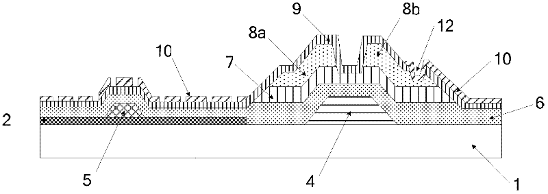
[0055] like figure 2 As shown, in this embodiment, the array substrate includes: a substrate 1; a common electrode 2 formed on the substrate; an insulating layer 3 covering the common electrode 2 and extending to the substrate 1, and the insulating layer 3 covering the common electrode 2 The first via hole 11 is opened in the part; the gate electrode 4 and the common electrode line 5 formed on the insulating layer 3, that is, the common electrode line 5 and the gate electrode 4 are arranged on the same layer, and the common electrode line 5 is located in the first via hole Above 11, the common electrode line 5 is connected to the common electrode 2 through the first via hole 11; the gate electrode protection layer (i.e. gate insulating layer) 6, the gate electrode protection layer 6 connects the gate electrode 4, the common electrode line 5 and the insulating layer 3 completely covered; the active layer 7 formed on the gate electrode protection layer 6; the source electrode 8...

Embodiment 2

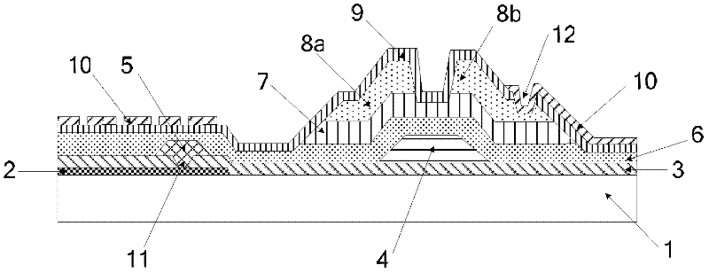
[0066] like image 3 As shown, in this embodiment, the array substrate includes: a substrate 1; a gate electrode 4 and a common electrode line 5 formed on the substrate 1, that is, the common electrode line 5 and the gate electrode 4 are arranged on the same layer; And cover the insulating layer 3 of the gate electrode 4 and the common electrode line 5, the part of the insulating layer 3 covering the common electrode line 5 has a first via hole 11, and the first via hole 11 is located above the common electrode line 5; The common electrode 2 formed on the insulating layer 3, the common electrode 2 is located above the first via hole 11, and the common electrode 2 is connected to the common electrode line 5 through the first via hole 11; completely covering the common electrode 2 and the insulating layer 3 Gate electrode protective layer 6; active layer 7 formed on gate electrode protective layer 6 above gate electrode 4; source electrode 8a and drain electrode 8b formed on act...

Embodiment 3

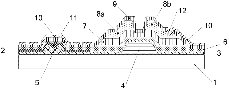
[0075] like Figure 4 As shown, in this embodiment, the array substrate includes: a substrate 1; a gate electrode 4 and a common electrode line 5 formed on the substrate 1, that is, the common electrode line 5 and the gate electrode 4 are arranged on the same layer; The insulating layer 3 that covers the gate electrode 4 and the common electrode line 5; the common electrode 2 formed on the insulating layer 3, the common electrode 2 is located above the common electrode line 5; the gate electrode that completely covers the common electrode 2 and the insulating layer 3 protective layer 6; an active layer 7 formed on the gate electrode protective layer 6 above the gate electrode 4; a source electrode 8a and a drain electrode 8b formed on the active layer 7; covering the source electrode 8a and the drain electrode 8b and extending to The passivation layer 9 on the gate electrode protection layer 6, the part of the passivation layer 9 covering the drain electrode 8b has a second vi...


PUM


Abstract

The invention provides an array substrate, comprising a substrate, a common electrode and a pixel electrode which are sequentially formed on the substrate and are mutually insulated, a thin film transistor, a common electrode wire and an insulating layer, wherein the thin film transistor comprises a gate electrode, an active layer, a source electrode and a drain electrode; the drain electrode is electrically connected with the pixel electrode, the common electrode wire is arranged at the same layer of the gate electrode, the insulating layer is arranged between the gate electrode and the common electrode and is used for isolating the gate electrode from the common electrode, and the common electrode is connected with the common electrode wire by virtue of a through hole of the insulating layer. Accordingly, the invention provides a manufacturing method of the array substrate and display equipment adopting the array substrate. The array substrate disclosed by the invention can overcome the defect that the aperture ratio of unit pixel is lower in the prior art.

Description

technical field [0001] The invention belongs to the technical field of display manufacturing, and in particular relates to an array substrate, a manufacturing method thereof, and a display device using the array substrate. Background technique [0002] With the development of display manufacturing technology, liquid crystal display technology has developed rapidly, and has gradually replaced traditional picture tube displays and become the mainstream of future flat panel displays. In the field of liquid crystal display technology, TFT-LCD (Thin Film Transistor Liquid Crystal Display, Thin Film Transistor Liquid Crystal Display) is widely used in televisions, computers, Mobile phones and other fields. [0003] Among them, the ADSDS (ADvanced Super Dimension Switch, referred to as ADS) type TFT-LCD has high resolution, high transmittance, low power consumption, wide viewing angle, high aperture ratio, low color difference, and no crowding. Advantages such as push Mura are wi...

Claims


Application Information

Patent Timeline
Patent Type & Authority Applications(China)
IPC IPC(8): G02F1/1362G02F1/1368H01L27/12H01L21/77
CPCG02F1/1368G02F1/136227G02F2201/40G02F1/136286G02F1/134318H01L27/1248H01L27/1214G02F1/1345H01L27/124H01L27/1218G02F1/133345G02F2201/121G02F2201/123H01L23/3171
Inventor 白金超刘耀李梁梁孙亮郝昭慧
Owner BOE TECH GRP CO LTD
Why Eureka
Try Eureka