Organic electroluminescence display device and manufacturing method thereof

An electroluminescence display and display device technology, applied in semiconductor/solid-state device manufacturing, circuits, electrical components, etc., can solve the problems of chromaticity variation, difficulty in mass production, and high cost of metal mask manufacturing, and achieve enhanced luminous efficiency. , Enhance the effect of color purity and chromaticity change suppression

Active Publication Date: 2016-04-06
JOLED INC
View PDF5 Cites 0 Cited by
  • Summary
  • Abstract
  • Description
  • Claims
  • Application Information

AI Technical Summary

Problems solved by technology

However, vacuum evaporation has disadvantages in that it is difficult to apply to large-screen substrates and vacuum evaporation is also difficult to use because it is difficult to properly use metal masks for deposition and the equipment and manufacturing costs are high especially when large-scale panels are manufactured. mass production
[0011] However, the organic EL element disclosed in the above-mentioned Japanese Patent Unexamined Publication No. 2006-140434 has problems in that the luminous efficiency of the light-emitting layer containing the phosphorescent light-emitting material actually decreases, and the chromaticity changes due to the current density dependence

Method used


Image

  • Organic electroluminescence display device and manufacturing method thereof
  • Organic electroluminescence display device and manufacturing method thereof
  • Organic electroluminescence display device and manufacturing method thereof

Examples


no. 1 approach ;

[0047] (Organic EL display device including a second light-emitting layer formed from a phosphorescent low-molecular material by a printing method)

[0048] the whole frame

[0049]Manufacturing method

[0050] 2. A variant of the first embodiment;

[0051] (Organic EL display device using a second light-emitting layer formed by a method other than the printing method)

no. 2 approach

[0052] 3. The second embodiment;

[0053] (Organic EL display device including a second light-emitting layer formed from a phosphorescent low-molecular material and a high-molecular material)

[0054] 4. The third embodiment; and

[0055] (Organic EL display device including a second light-emitting layer formed from a phosphorescent low-molecular material)

[0056] 5. Application examples.

no. 1 approach

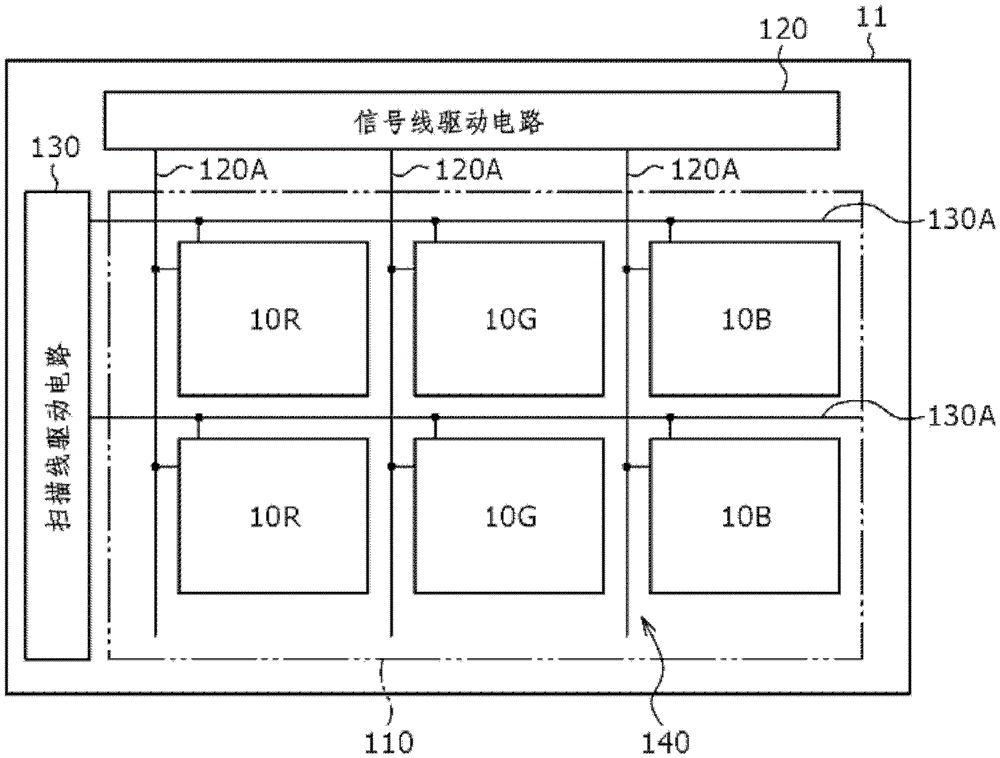
[0058] figure 1 is a block diagram showing the structure of the organic EL display device 1 according to the first embodiment of the present invention. The organic EL display device 1 is used in organic EL televisions and the like. For example, in the organic EL display device 1, a plurality of red organic EL elements 10R, a plurality of green organic EL elements 10G, and a plurality of blue organic EL elements 10B, which will be described later, are arranged in a matrix form in a display area 110 on a substrate 11. middle. Around the display area 110, a signal line driver circuit 120 and a scan line driver circuit 130 are provided as drivers for screen display.

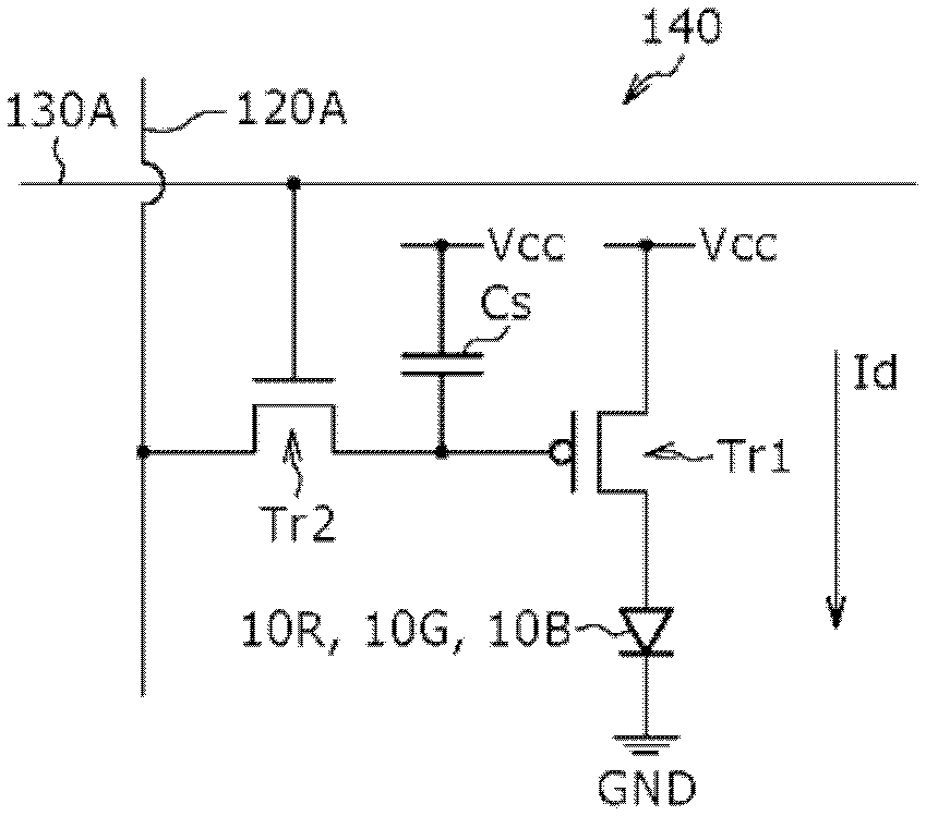
[0059] A pixel drive circuit 140 is provided in the display region 110 . figure 2 It is a circuit diagram showing a part of the configuration of the pixel driving circuit 140 . The pixel driving circuit 140 is an active type driving circuit formed in a lower layer of the lower electrode 14 to be described later....


PUM


Abstract

The invention discloses an organic EL display device capable of enhancing luminous efficiency without changing chromaticity and a manufacturing method thereof. The organic EL display device comprises: a lower electrode arranged on a substrate corresponding to a blue first organic EL element and a second organic EL element of other colors; The hole injection / transport layer provided for the EL element; the second organic light-emitting layer of other colors arranged on the hole injection / transport layer for the second organic EL element; the second organic light-emitting layer and the first organic EL element a connection layer made of a low molecular material provided on the entire surface of the hole injection / transport layer; a blue first organic light-emitting layer provided on the entire surface of the connection layer; and a first organic light-emitting layer on the first organic light-emitting layer An electron injection / transport layer and an upper electrode are sequentially provided on the entire surface.

Description

[0001] Cross References to Related Applications [0002] The present invention contains subject matter related to Japanese Priority Patent Application JP2011-048353 filed in Japan Patent Office on Mar. 4, 2011, the entire content of which is hereby incorporated by reference. technical field [0003] The present invention relates to an organic electroluminescence (EL) display device and a manufacturing method thereof, wherein the organic EL display device emits light by utilizing the organic EL phenomenon. Background technique [0004] With the accelerated development of the information and communication industry, higher performance display elements are required. In particular, an organic EL element attracting attention as a next-generation display device has not only advantages of a wide viewing angle and excellent contrast ratio but also an advantage of fast response time in a self-luminous type display device. [0005] Materials used in light emitting layers and the like ...

Claims


Application Information

Patent Timeline
Patent Type & Authority Patents(China)
IPC IPC(8): H01L27/32H01L51/50
CPCH10K59/35H10K50/13H10K50/15H10K50/11H10K2101/10H01L2924/01077H10K50/00H10K50/17H10K71/00
Inventor 吉永祯彦松元寿树肥后智之
Owner JOLED INC
Why Eureka
Try Eureka