Method for manufacturing semiconductor device

A manufacturing method and semiconductor technology, applied in the fields of semiconductor/solid-state device manufacturing, semiconductor devices, electrical components, etc., can solve the problems of current leakage, many crystal defects, uncontrollable impurity pattern shape, etc., and achieve the effect of less crystal defects

Inactive Publication Date: 2012-09-12
HITACHI LTD
View PDF12 Cites 5 Cited by
  • Summary
  • Abstract
  • Description
  • Claims
  • Application Information

AI Technical Summary

Problems solved by technology

Therefore, there are the following disadvantages: there are many crystal defects, it is easy to cause a current leakage path, and the shape of the impurity map cannot be controlled (even if the pn junction is made on the back side, it will all be mixed)

Method used


Image

  • Method for manufacturing semiconductor device
  • Method for manufacturing semiconductor device
  • Method for manufacturing semiconductor device

Examples


Embodiment 1

[0035] Embodiment 1 will be described in detail below with reference to the drawings.

[0036] (Manufacturing method of IGBT)

[0037] refer to Figure 1 to Figure 10 A method of manufacturing an IGBT will be described. In particular, the description will focus on the method of forming the field stop layer and the collector layer.

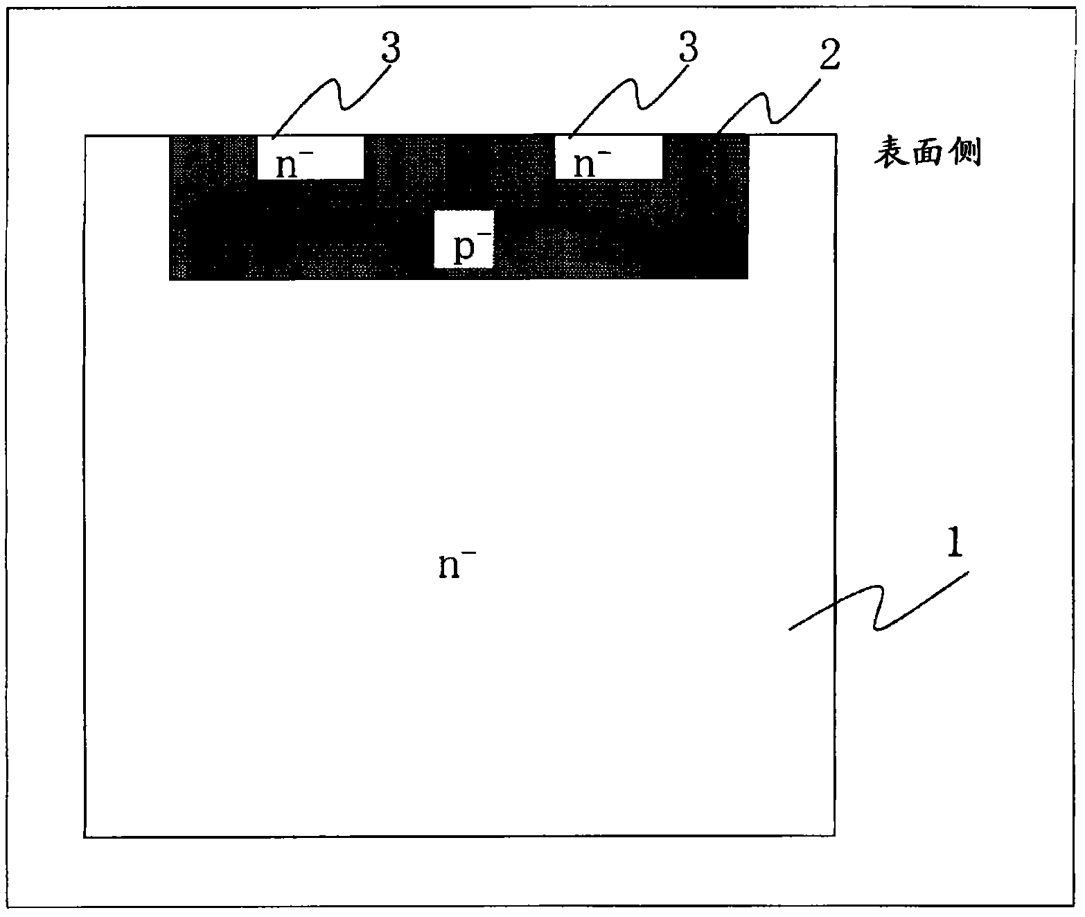
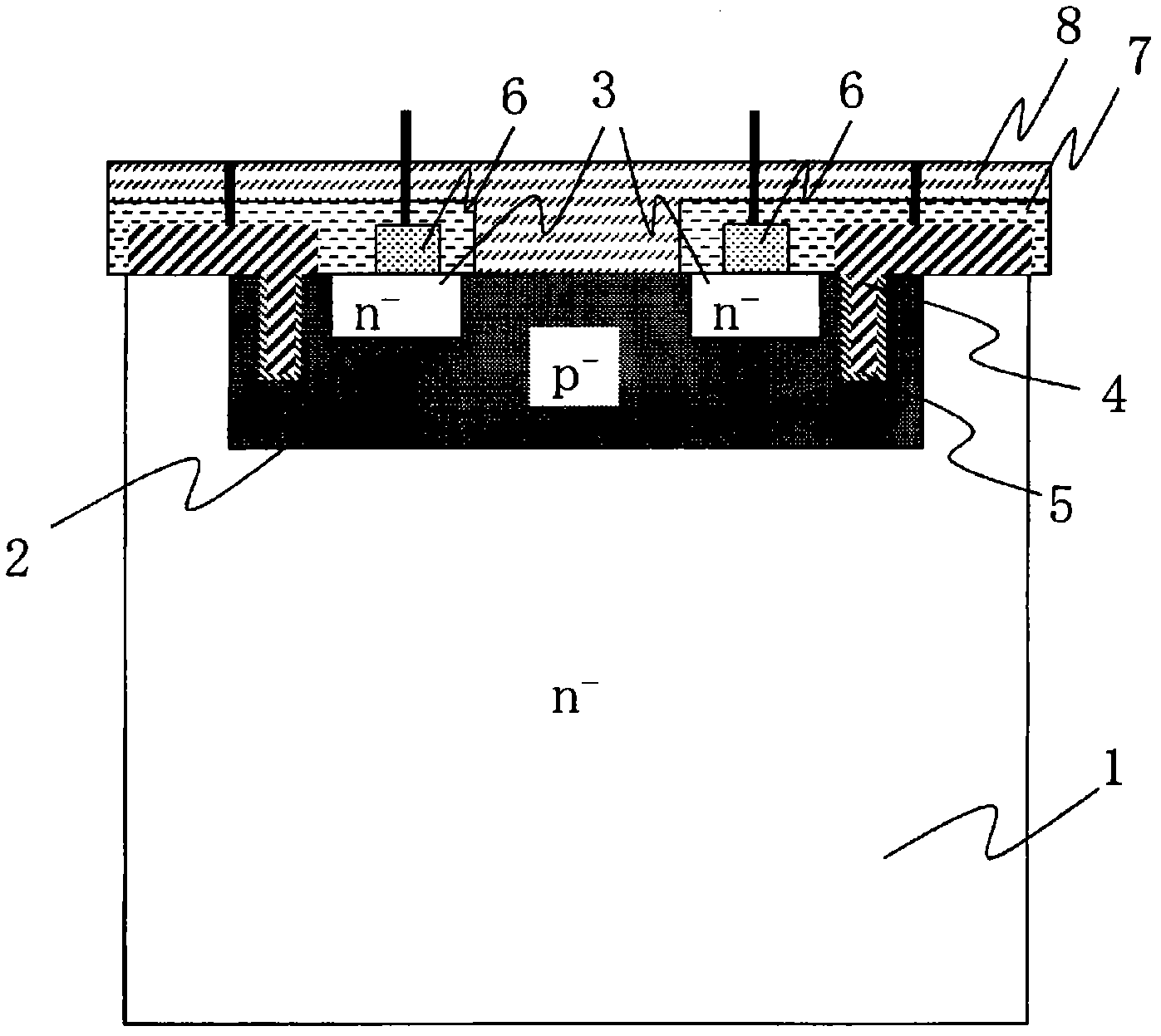
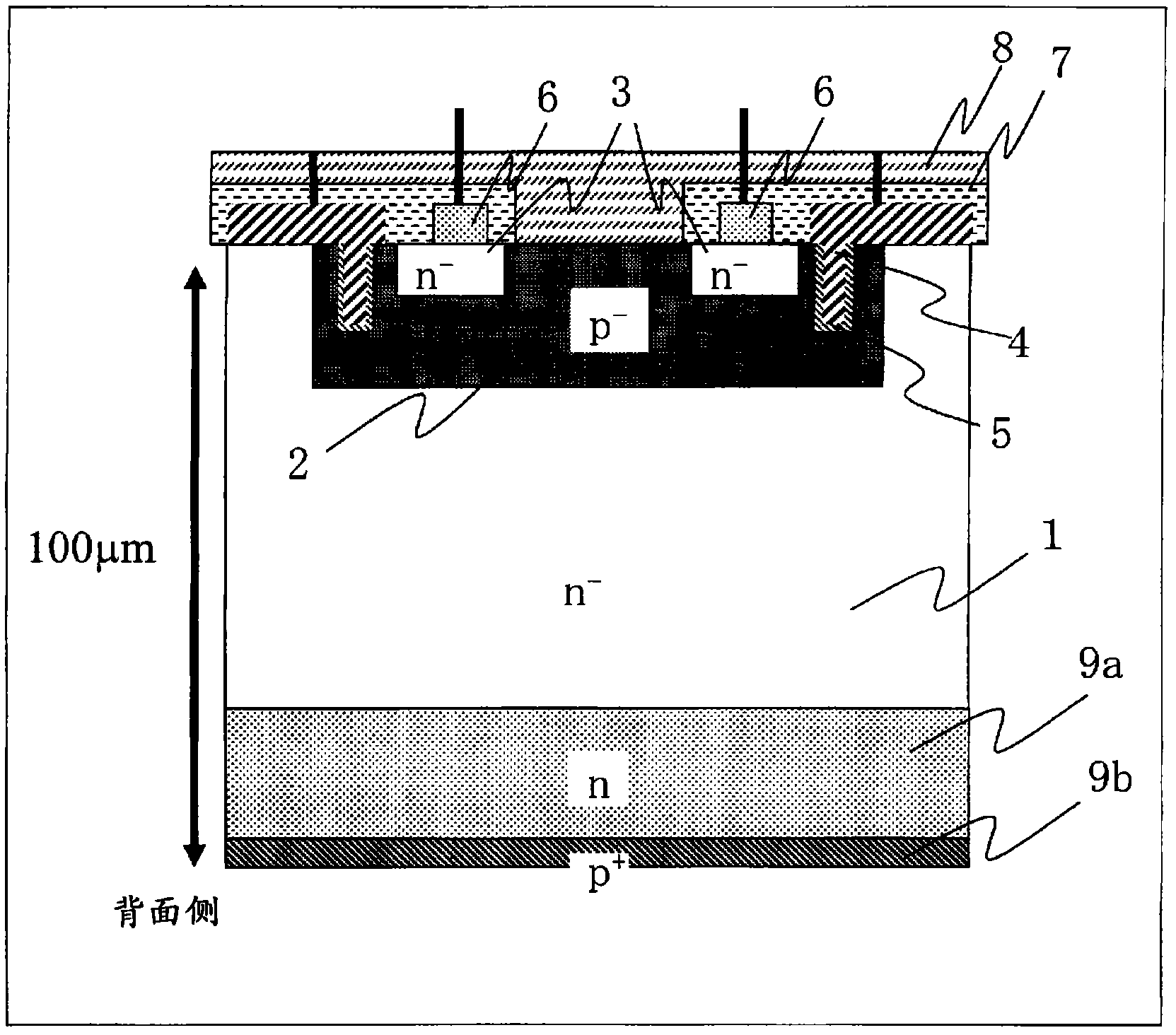
[0038] figure 1 A cross-sectional view of the main body schematically showing the manufacturing process of the IGBT 100 . IGBT 100 is formed using n-type silicon single crystal wafers (CZ, MCZ, FZ). IGBT100 has formed in n - The p-type body layer 2 on the type drift layer 1, and the n-type body layer formed on the surface part of the body layer 2 + Type source region 3. The body layer 2 and the source region 3 can be formed on the surface of the drift layer 1 by ion implantation technology.

[0039] Next, if figure 2 As shown, trench gate 4 is formed on IGBT100. The trench gate 4 is opposed to the body layer 2 via the gate insulating fil...


PUM

PropertyMeasurementUnit
thicknessaaaaaaaaaa
wavelengthaaaaaaaaaa

Abstract

Disclosed is a method for manufacturing a semiconductor device, wherein a semiconductor Si substrate, which is thinned down to 300 [mu]m or less, is heated such that the temperature at a position deeper than 1 [mu]m from the back surface of the semiconductor Si substrate is within a temperature range of 950-1412 DEG C (inclusive) without melting Si during a laser annealing process. Specifically disclosed is a method for manufacturing a semiconductor device, wherein a semiconductor region is formed by introducing an impurity from the front surface of a semiconductor substrate, the substrate is fixed to a supporting substrate using an electrostatic chuck, and then the impurity is activated by heating the front surface of the substrate by irradiation of a laser having a long wavelength of 3 [mu]m or more, while heating the entire substrate at 250 DEG C or more.

Description

technical field [0001] The present invention relates to a laser annealing technique used for activating impurities introduced into a semiconductor substrate, and to a method of manufacturing a semiconductor device using the impurity activation method. Background technique [0002] An extremely thin IGBT (Insulated Gate Bipolar Transistor, Insulated Gate Bipolar Transistor) in which the thickness of Si is reduced to about 100 μm is known. The ultra-thin IGBT has n + type field termination layer and p + type collector layer. Usually, the field stop layer and the collector layer are formed in a laminated manner. The field stop layer and the collector layer can be obtained by introducing phosphorus ions as an n-type impurity to a deep position from the back surface of the semiconductor substrate, and introducing boron ions as a p-type impurity to a shallow position, and then performing heat treatment for activation. [0003] As the above heat treatment method, laser anneali...

Claims


Application Information

Patent Timeline
Patent Type & Authority Applications(China)
IPC IPC(8): H01L21/265H01L21/336H01L29/739H01L29/78
CPCH01L21/268H01L21/324H01L21/6831H01L29/66348H01L29/7397
Inventor 岛明生朴泽一幸
Owner HITACHI LTD
Why Eureka
Try Eureka