Film coating part and preparation method thereof
A technology for coating parts and magnetron sputtering coating, applied in the field of coating parts and their preparation, can solve the problems of limiting the application range of PVD of aluminum alloy substrates, large thermal expansion coefficient, and easy falling off of the film layer, so as to improve the service life and additional value, enhance competitiveness, and avoid the effect of weak cohesion
- Summary
- Abstract
- Description
- Claims
- Application Information
AI Technical Summary
Problems solved by technology
Method used
Image
Examples
preparation example Construction
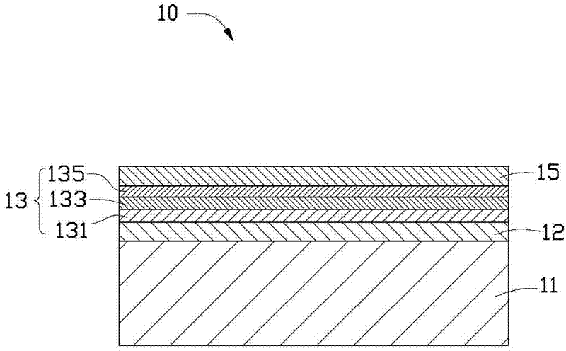
[0024] The preparation method of the coating member 10 in the preferred embodiment of the present invention includes the following steps:
[0025] An aluminum alloy base 11 is provided, and the aluminum alloy base 11 is pre-treated. The pretreatment may include: successively wiping the surface of the aluminum alloy substrate 11 with deionized water and absolute ethanol, and placing the aluminum alloy substrate 11 in an ultrasonic cleaner containing an acetone solution for ultrasonic cleaning to remove the aluminum alloy substrate 11 Impurities and oil stains on the surface.
[0026] Plasma cleaning is performed on the surface of the aluminum alloy substrate 11 after the pretreatment to further remove dirt on the surface of the aluminum alloy substrate 11 and improve the bonding force between the surface of the aluminum alloy substrate 11 and the subsequent coating.
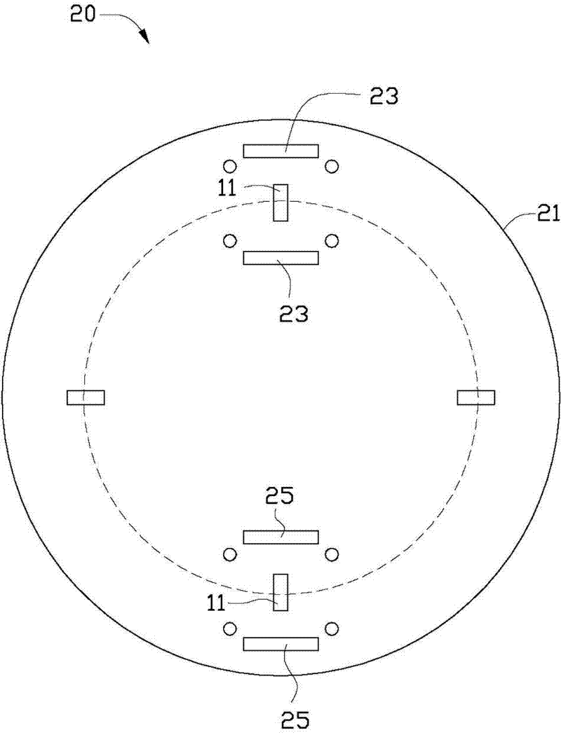
[0027] See figure 2 , Put the aluminum alloy substrate 11 into the coating chamber 21 of a vacuum sputtering machine...
Embodiment 1
[0041] Plasma cleaning: The flow of argon gas is 280sccm, the bias voltage of the aluminum alloy substrate 11 is -300V, and the plasma cleaning time is 9 minutes;
[0042] Sputtered aluminum layer 12: Ar gas flow rate is 150 sccm, the bias voltage of the aluminum alloy substrate 11 is -200V, the sputtering temperature is 30°C, the sputtering time is 20 minutes, and the thickness of the aluminum layer 12 is 120 nm;
[0043] Sputtering the first AlON layer 131: Argon flow rate is 150 sccm, nitrogen flow rate is 20 sccm, oxygen flow rate is 20 sccm, the bias voltage of the aluminum alloy substrate 11 is -200V, the sputtering temperature is 30°C, and the sputtering time is 30 minutes. The thickness of an AlON layer 131 is 130 nm, the atomic percentage of Al is 70 at.%, O is 15 at.%, and N is 15 at.%;
[0044] Sputtering the second AlON layer 133: Argon flow rate is 150 sccm, nitrogen flow rate is 40 sccm, oxygen flow rate is 40 sccm, the bias voltage of the aluminum alloy substrate 11 is...
Embodiment 2
[0048] Plasma cleaning: The flow of argon gas is 280sccm, the bias voltage of the aluminum alloy substrate 11 is -300V, and the plasma cleaning time is 7 minutes;
[0049] Sputtering aluminum layer 12: the flow of argon is 200 sccm, the bias voltage of the aluminum alloy substrate 11 is -200V, the sputtering temperature is 50°C, the sputtering time is 30 minutes, and the thickness of the aluminum layer 12 is 180 nm;
[0050] Sputtering the first AlON layer 131: Argon flow rate is 200 sccm, nitrogen flow rate is 25 sccm, oxygen flow rate is 25 sccm, the bias voltage of the aluminum alloy substrate 11 is -100V, the sputtering temperature is 50°C, and the sputtering time is 40 minutes. The thickness of an AlON layer 131 is 150 nm, the atomic percentage of Al is 65 at.%, O is 18 at.%, and N is 17 at.%;
[0051] Sputtering the second AlON layer 133: Argon flow rate is 200 sccm, nitrogen flow rate is 45 sccm, oxygen flow rate is 45 sccm, the bias voltage of the aluminum alloy substrate 11 ...
PUM
| Property | Measurement | Unit |
|---|---|---|
| thickness | aaaaa | aaaaa |
| thickness | aaaaa | aaaaa |
| thickness | aaaaa | aaaaa |
Abstract
Description
Claims
Application Information


