Film LED (light-emitting diode) chip device as well as manufacturing method and application thereof

A device manufacturing method and LED chip technology, applied to semiconductor devices, electrical components, circuits, etc., can solve the problems of increased production costs, changes, lack of effective support and heat sinks, etc.

Active Publication Date: 2015-07-22
ELEC TECH PHOTOELECTRIC TECH DALIAN
View PDF3 Cites 0 Cited by
  • Summary
  • Abstract
  • Description
  • Claims
  • Application Information

AI Technical Summary

Problems solved by technology

[0003] see figure 1 , the traditional thin-film LED chip device has the following problems: there are unfilled gaps 4 between the metal bumps 2 used to combine the GaN epitaxial layer film 1 and the flip-chip substrate 3 in the flip-chip structure chip, and the GaN epitaxial layer film 1 is partially lacking Effective support and heat sink, so that it is easy to cause chip cracking or structural change due to instantaneous mechanical vibration or instantaneous thermal effect during the laser lift-off process, resulting in failure, which eventually leads to low yield of thin-film LED chip devices
[0004] see figure 2 , the traditional thin-film LED chip device needs to separate the chip from the substrate 5 one by one during the laser lift-off process. This process is slow and time-consuming, and it is not easy to achieve mass production; The unit separation before the process divides the substrate into smaller individuals, and the stripped substrate cannot be recycled and reused, resulting in waste of resources and increased production costs

Method used


Image

  • Film LED (light-emitting diode) chip device as well as manufacturing method and application thereof
  • Film LED (light-emitting diode) chip device as well as manufacturing method and application thereof
  • Film LED (light-emitting diode) chip device as well as manufacturing method and application thereof

Examples


Embodiment Construction

[0067] Below in conjunction with accompanying drawing and specific embodiment the present invention will be further described:

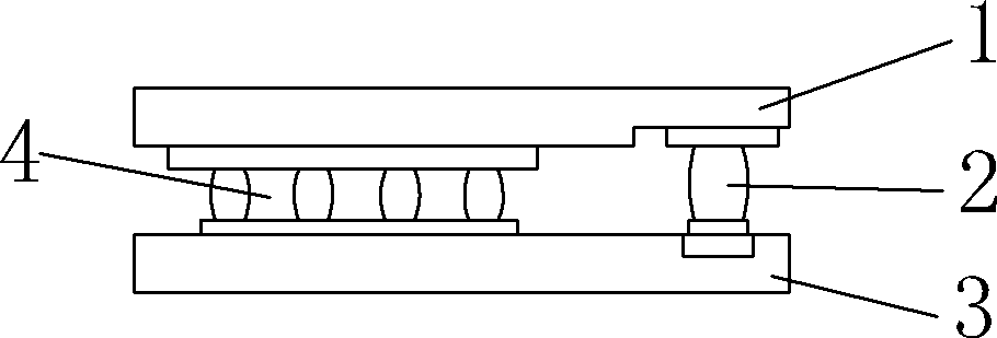
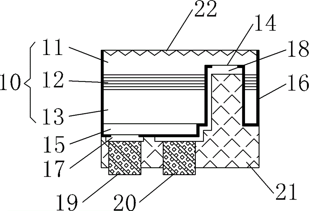
[0068] see image 3 , the thin film LED chip device, comprising:

[0069] A GaN-based epitaxial film base layer 10 composed of an N-type semiconductor layer 11, an active layer 12, and a P-type semiconductor layer 13 in sequence. In order to improve the external quantum efficiency of the thin film LED chip device made, the surface of the N-type semiconductor layer 11 is a roughened surface 22; or, a passivation layer (not shown) is deposited on the surface of the N-type semiconductor layer 11, The passivation layer is SiO 2 or Si 3 N 4 The material has a thickness of 0.1 μm-1500 μm.

[0070] The etching groove 14 extends along the surface of the P-type semiconductor layer 13 to the N-type semiconductor layer 11 .

[0071] The surface of the P-type semiconductor layer 13 is attached with a metal reflective layer 15 in ohmic contact with it.

[...


PUM

PropertyMeasurementUnit
thicknessaaaaaaaaaa
depthaaaaaaaaaa
widthaaaaaaaaaa

Abstract

The invention provides a film LED (light-emitting diode) chip device, comprising a GaN-based epitaxial film base which is provided with an etching groove, and a fixed film which is coated on a GaN-based epitaxial film, wherein a metal reflection layer is attached to the surface of the P-shaped semiconductor layer of the GaN-based epitaxial film base, passive films are deposited on the metal reflection layer and the GaN-based epitaxial film base to form the GaN-based epitaxial film, the passive film on the surface of the metal reflection layer and the passive film on the bottom surface of the etching groove are respectively provided with a hollowed-out area, a P pole multilayer metal bonding layer and a N pole multilayer metal bonding layer are respectively arranged on the corresponding hollowed-out area, and a P pole conductive support thick metal layer and an N pole conductive support thick metal layer are respectively arranged on the P pole multilayer metal bonding layer and the N pole multilayer metal bonding layer. The invention also provides a manufacturing method and application of the film LED chip device. According to the invention, the occurrence rate of wafer fracture and the probability of wafer deformation in the subsequent laser stripping process are reduced, and the yield of products is improved.

Description

technical field [0001] The invention relates to the technical field of LEDs, in particular to a thin-film LED chip device and its manufacturing method and application. Background technique [0002] Existing thin-film LED chip devices use excimer laser lift-off substrate technology to peel off the substrate (sapphire substrate or SiC substrate) growing GaN materials on the basis of traditional flip-chip structure chips, exposing the LED thin-film structure . [0003] see figure 1 , the traditional thin-film LED chip device has the following problems: there are unfilled gaps 4 between the metal bumps 2 used to combine the GaN epitaxial layer film 1 and the flip-chip substrate 3 in the flip-chip structure chip, and the GaN epitaxial layer film 1 is partially lacking Effective support and heat sink, so that it is easy to cause chip cracking or structural change due to instantaneous mechanical vibration or instantaneous thermal effect during the laser lift-off process, resultin...

Claims


Application Information

Patent Timeline
Patent Type & Authority Patents(China)
IPC IPC(8): H01L33/00H01L33/62
Inventor 王冬雷林惠雄
Owner ELEC TECH PHOTOELECTRIC TECH DALIAN
Why Eureka
Try Eureka