
Method for reducing HCI effect of I/O MOS device

An effect and device technology, applied in the field of reducing the HCI of I/O MOS devices, to achieve the effects of reducing the HCI effect, increasing the LDD diffusion, and reducing the lateral electric field strength

Active Publication Date: 2012-09-26
SEMICON MFG INT (SHANGHAI) CORP
View PDF3 Cites 0 Cited by
  • Summary
  • Abstract
  • Description
  • Claims
  • Application Information

AI Technical Summary

Problems solved by technology

[0005] Therefore, it is not enough to improve the HCI effect simply by changing the dose and energy of LDD ion implantation

Method used


Image

  • Method for reducing HCI effect of I/O MOS device
  • Method for reducing HCI effect of I/O MOS device
  • Method for reducing HCI effect of I/O MOS device

Examples


Embodiment Construction

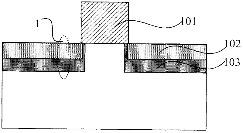
[0028] The method for reducing the hot carrier injection effect of the I / O MOS device proposed by the present invention will be further described in detail below in conjunction with the accompanying drawings and specific embodiments. Advantages and features of the present invention will be apparent from the following description and claims. It should be noted that all the drawings are in very simplified form, and are only used for the purpose of conveniently and clearly assisting in describing the embodiments of the present invention.

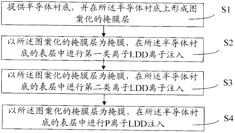
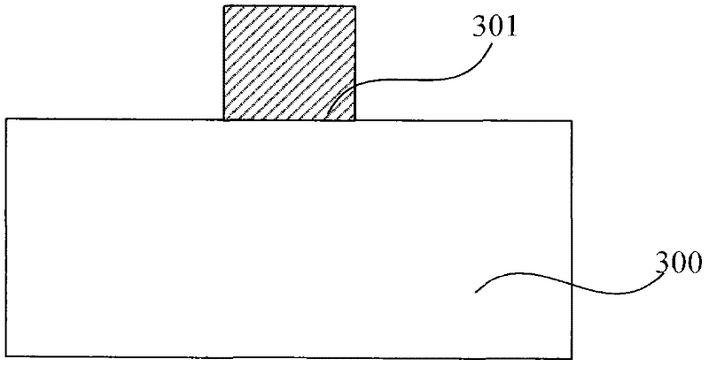
[0029] Such as figure 1 As shown, the present invention provides a method for reducing the hot carrier injection effect of I / O NMOS devices, which is completed by the steps shown in S1 to S3, combined below figure 2 The process flow diagram shown and Figure 3A-3D The schematic diagram of the cross-sectional structure of the process is described in detail for the above-mentioned method.

[0030] S1, providing a semiconductor substrate, and ...


PUM


Abstract

The invention provides a method for reducing an HCI effect of an I / O MOS device. The method comprises the steps of providing a semiconductor substrate and forming a patterned mask layer on the semiconductor substrate; carrying out an LDD ion implantation of a first ion in a surface layer of the semiconductor substrate using the patterned mask layer as a mask; carrying out an LDD ion implantation of a second ion in the surface layer of the semiconductor substrate using the patterned mask layer as a mask, the second ion having an opposite conductive type to that of the first ion; and carrying out an LDD ion implantation of a phosphor ion in the surface layer of the semiconductor substrate using the patterned mask layer as a mask. According to the method of the invention, SCE and HCI effects can be improved through the triple LDD ion implantations of the first ion, the second ion and the phosphor ion, and with no need of adding extra mask layers; and simultaneously good electric properties of MOS device can be maintained.

Description

technical field [0001] The invention relates to the field of semiconductor manufacturing, in particular to a method for reducing HCI of an I / O MOS device. Background technique [0002] In today's integrated circuits, input / output (I / O) devices are an important component. Compared with core devices, I / O devices feature high operating voltage and high drive capability. However, under high operating voltage, the channel of the I / O device has a strong lateral electric field, which causes the impact ionization of the carriers during the transport process, generating additional electron-hole pairs, and part of the hot carriers are injected into the gate oxide layer. , so that the threshold voltage of the device increases, the saturation current and carrier mobility decrease, etc. This phenomenon is called the HCI (Hot Carrier Injection) effect. The HCI effect is a problem often encountered in the design of I / O devices, and it is the main factor affecting the characteristics and ...

Claims


Application Information

Patent Timeline
Patent Type & Authority Applications(China)
IPC IPC(8): H01L21/266H01L21/336
CPCH01L29/7833H01L29/6659H01L29/0847H01L29/167
Inventor 赵猛
Owner SEMICON MFG INT (SHANGHAI) CORP
Learn More