Organic electroluminescent device

An electroluminescent device and electroluminescent technology, which is applied in the direction of electro-solid devices, luminescent materials, electrical components, etc., can solve the problems of reduced device repeatability, affected device performance, material absorption loss, etc., so as to reduce luminous loss and improve light The effect of emissivity

Active Publication Date: 2012-09-26
OCEANS KING LIGHTING SCI&TECH CO LTD +1
View PDF10 Cites 18 Cited by
  • Summary
  • Abstract
  • Description
  • Claims
  • Application Information

AI Technical Summary

Problems solved by technology

However, since OLEDs generally have a multi-layer structure, and the electrodes generally use metal electrodes, when the device emits light, it will cause low luminous efficiency due to various light losses, such as: emission loss, light absorption by materials loss etc.
Even if the recombination rate of electrons and holes reaches 100%, due to these losses, the light used for luminescence is very little. Studies have shown that in current devices, the real emitted light only accounts for 25% of the total luminescence. %, therefore, how to design the device more reasonably to make the light output as much as possible is one of the current research hotspots. If the problem of light output is solved, then the luminous efficiency of OLED will usher in a leap in performance
[0004] Among the traditional light-emitting devices, the most researched is the bottom-emitting device structure, with the ITO glass substrate as the light-emitting surface. This kind of device has mature technology and has been studied a lot. However, because the light will first go through the absorption and reflection of the ITO conductive material , the glass needs to be absorbed and reflected again. Therefore, the light emission rate is very low, and most of the light is lost. To increase the light emission rate of this type of device, the shape of the exit surface substrate needs to be modified. To improve the luminous efficiency, the process increases and the processing is complicated; at the same time, the most research on light emission is to increase the light emission by adding different anti-reflection coatings, and rarely consider the refractive index matching between organic layers. , the feature is that in the multi-layer structure, the absorption and refraction of light by various organic layer materials is a problem worthy of attention; at the same time, the more organic layers, the thicker the device, the more reflection between layers, and at the same time , the factors affecting the performance of the device increase, and the preparation defects of each layer directly affect the performance of the device, making processing difficult and reducing the repeatability of the device

Method used


Image

  • Organic electroluminescent device
  • Organic electroluminescent device
  • Organic electroluminescent device

Examples


preparation example Construction

[0038] The preparation method of the above-mentioned organic electroluminescence device comprises the following steps:

[0039] (1) First, ultrasonically treat the glass substrate with detergent, acetone, ethanol and isopropanol for 15 minutes respectively;

[0040] (2) Prepare a layer of reflective layer with a thickness of 50-200nm on one side of the glass substrate in (1). The preparation method includes various suitable methods, such as evaporation, sputtering, spraying, chemical evaporation deposition, electrochemical method etc., preferably sputtering;

[0041] (3) Then prepare a conductive film with a thickness of 70-200nm on the other side of the glass substrate. The preparation method includes various suitable methods, such as evaporation, sputtering, spraying, chemical evaporation deposition, electrochemical methods, etc., Preferably sputtering;

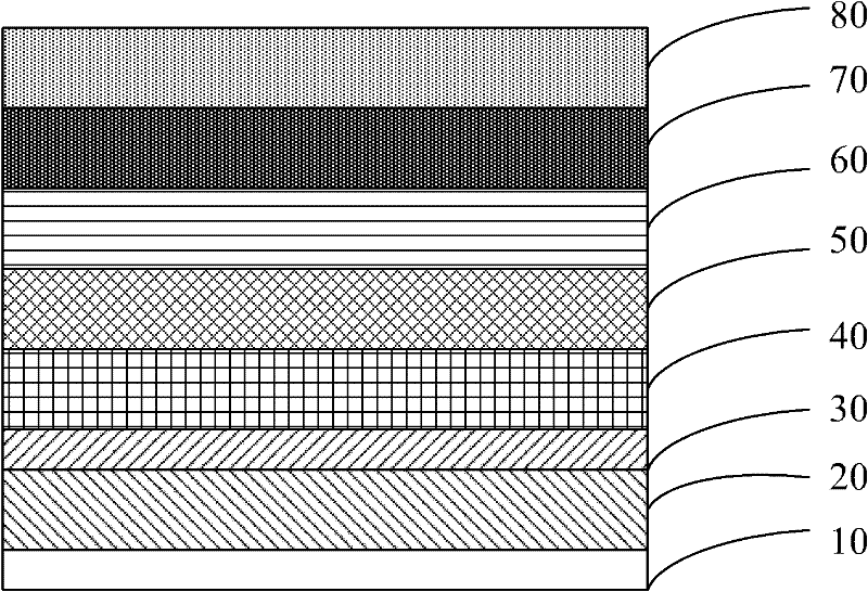
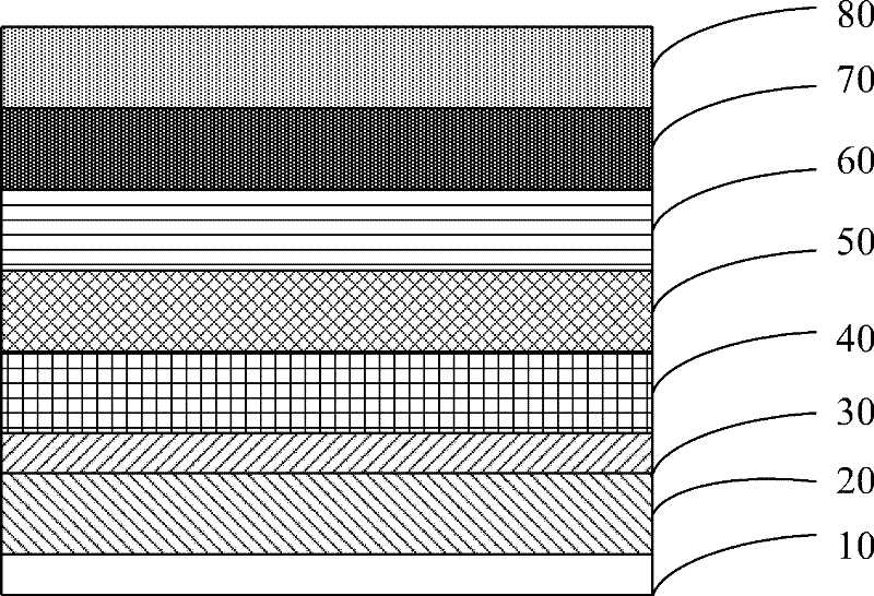
[0042] (4) A cathode, an n-type doped electron transport layer, a p-n type doped light-emitting layer, a p-type hole tr...

Embodiment 1

[0045] Example 1: Firstly, the glass is ultrasonicated with detergent, acetone, ethanol and isopropanol for 15 minutes respectively, then a layer of Ag with a thickness of 100 nm is evaporated on one side of the glass substrate, and then a layer of Ag is sputtered on the other side of the glass ITO conductive film with a thickness of 120nm, 150nm of Ag and 40nm of n-type doped TPBi / Cs are sequentially evaporated on the side with the conductive film 2 CO 3 , where Cs 2 CO 3 The doping ratio of 10%; 30nm doped light-emitting layer TPBi / NPB / DCJTB, wherein the mass ratio of NPB to TPBi is 1:1, the doping ratio of luminescent material is 5%; 40nm p-type doped MoO 3 / NPB, where MoO 3 The doping ratio is 30%; finally, a layer of Ag with a thickness of 120nm is vapor-deposited.

Embodiment 2

[0046] Example 2: Firstly, the glass is ultrasonicated with detergent, acetone, ethanol and isopropanol for 15 minutes respectively, and then a layer of Ag with a thickness of 50 nm is evaporated on one side of the glass substrate, and then a layer of Ag is sputtered on the other side of the glass ITO conductive film with a thickness of 150nm, 200nm of Ag and 40nm of n-type doped TPBi / Cs are sequentially evaporated on the side with the conductive film 2 CO 3 , where Cs 2 CO 3 The doping ratio of 5%; 30nm doped luminescent layer TPBi / NPB / DCJTB, wherein the mass ratio of NPB to TPBi is 1:1, the doping ratio of luminescent material is 3%; 30nm p-type doped MoO 3 / NPB, where MoO 3 The doping ratio is 25%; finally, a layer of Ag with a thickness of 100nm is vapor-deposited.


PUM

PropertyMeasurementUnit
luminanceaaaaaaaaaa
luminous efficiencyaaaaaaaaaa
thicknessaaaaaaaaaa

Abstract

An organic electroluminescent device comprises a reflecting layer, a glass substrate, a conductive film, a metal cathode, an n-doped electron transport layer, a p-n doped luminescent layer, a p-doped hole transport layer and a metal anode which are orderly stacked together. The organic electroluminescent device is a top-emitting device of an inverse structure; lights are emitted from the top of the device, and the glass substrate equipped with the conductive film acts as a backlight surface, thus the problems of light absorption by the substrate and light emission from the substrate are well solved. In addition, the inverse structure enables the refractive index of materials to be arranged from small to big based on the direction of emitted light, and total reflection will not occur for the light at the moment, thus reducing light emission loss caused by total reflection and improving light exitance.

Description

【Technical field】 [0001] The invention relates to an organic electroluminescent device. 【Background technique】 [0002] In 1987, C.W.Tang and Van Slyke of Eastman Kodak Company in the United States reported a breakthrough in the research of organic electroluminescence. A high-brightness, high-efficiency double-layer small-molecule organic electroluminescent device was prepared using ultra-thin film technology. In the device with double-layer structure, the luminance reaches 1000cd / m2 at 10V, the luminous efficiency is 1.51lm / W, and the lifetime is more than 100 hours. In 1990, Burronghes et al. of the University of Cambridge proposed for the first time to use polymer conjugated polymer polyphenylene vinylene (PPV) to make polymer electroluminescence (EL) devices. Subsequently, the experimental group led by Professor Heeger of the University of California in the United States In 1991, the electroluminescent properties of polymers were further confirmed and improved. Since ...

Claims


Application Information

Patent Timeline
Patent Type & Authority Applications(China)
IPC IPC(8): H01L51/50H01L51/54C09K11/06
Inventor 周明杰王平黄辉陈吉星
Owner OCEANS KING LIGHTING SCI&TECH CO LTD
Why Eureka
Try Eureka