

Liquid crystal display panel, method for producing same and display device
A liquid crystal panel and liquid crystal layer technology, applied in the direction of instruments, nonlinear optics, optics, etc., can solve the problems of unstable thickness of liquid crystal cells and lower display quality, improve yield and display quality, reduce edge MURA, eliminate water ripple effect
- Summary
- Abstract
- Description
- Claims
- Application Information
AI Technical Summary
Problems solved by technology
Method used
Image

Examples
preparation example Construction
[0065] Wherein, the preparation method of the liquid crystal panel comprises the steps of:
[0066] Prepare a color filter substrate and an array substrate, wherein spacers and isolation frames are formed on the color filter substrate or the array substrate, and the spacers and / or the isolation frames are made of piezoelectric materials;
[0067] forming a liquid crystal layer on the color filter substrate or the array substrate;
[0068] Comparing the color filter substrate and the array substrate, wherein the spacer, the spacer frame and the liquid crystal layer are located between the color filter substrate and the array substrate, through the spacer and The isolation frame maintains a certain thickness of the liquid crystal layer, and isolates the liquid crystal layer and the sealing glue through the isolation frame to prevent contamination of the liquid crystal.
[0069] Taking the spacer and the isolation frame both as piezoelectric materials as an example, when the spa...
example 1
[0071] Example 1, the piezoelectric material columnar spacer and the isolation frame are prepared on the color filter substrate, with reference to Figures 1 to 9, including the following steps:
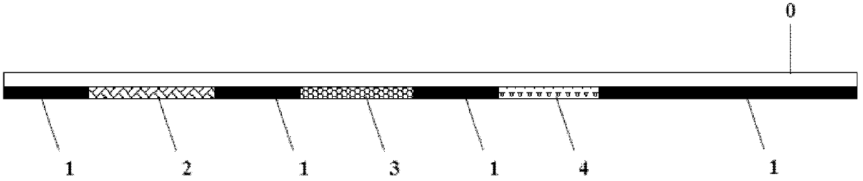
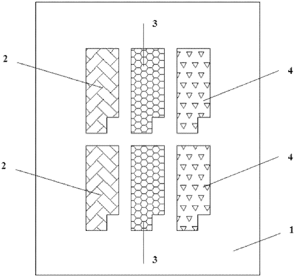
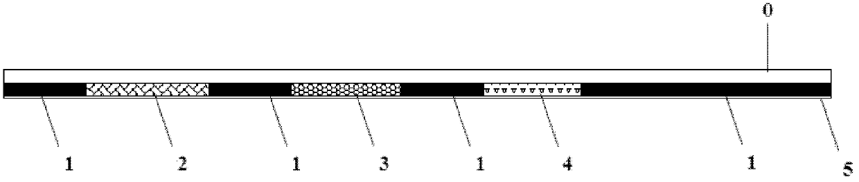
[0072] Step 1, prepare the color filter substrate (including making black matrix 1 and color pixels (R pixel 2, G pixel 3 and B pixel 4) on the glass substrate 0), such as Picture 1-1 , as shown in 1-2;
[0073] Step 2, deposit an insulating layer 5 on the substrate after step 1, such as figure 2 shown; those skilled in the art can understand that if the black matrix and the color pixel layer are non-conductive materials, then step 2 can be omitted;
[0074] Step 3, forming a first conductive layer on the color filter substrate after step 2 (the conductive layer can be a metal material or a transparent conductive material (indium tin oxide, zinc tin oxide, etc.) or other conductive materials), wherein the first conductive layer is formed Deposition, coating, sputtering or other fil...
example 2
[0087] Example 2, piezoelectric material columnar spacers and isolation frames are prepared on the array substrate, as shown in Figures 10 to 17, including the following steps:
[0088]Step 1, preparing the array substrate (including preparing the gate signal line metal layer 12, the gate insulating layer 13, the active layer, the source and drain electrodes, the data signal line metal layer 14, the passivation layer 15, and the silicon island on the glass substrate 0 16, pixel electrode layer 17, etc.), such as Figure 10-1 , as shown in 10-2;
[0089] Step 2, forming an insulating layer 53 on the prepared array substrate (such as by deposition or coating), such as Figure 11 shown;
[0090] Step 3, forming a first conductive layer on the array substrate after step 2 (for example, by depositing, coating or sputtering, etc., the conductive layer can be a metal material or a transparent conductive material (indium tin oxide, zinc tin oxide) or other Conductive material); thr...
PUM
 Abstract
Description
Claims
Application Information