Mold array process method for covering side edge of substrate
An array processing and substrate technology, which is applied in the field of packaging manufacturing, can solve problems such as the protection of the sealing body 130, adverse effects, and the inability of the side 116 to achieve the effect of avoiding exposure and improving durability
- Summary
- Abstract
- Description
- Claims
- Application Information
AI Technical Summary
Problems solved by technology
Method used
Image

Examples
no. 1 Embodiment
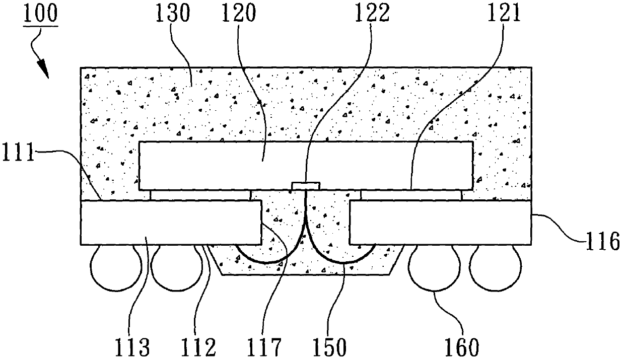
[0034] According to the first embodiment of the present invention, a molding array processing method covering the side of the substrate is exemplified in image 3A schematic cross-sectional view showing the structure of the semiconductor package made by it, Figure 4A to Figure 4F The cross-sectional schematic diagram of the components in each step and Figure 5 A partial top view of its substrate strip is shown. The details are as follows.
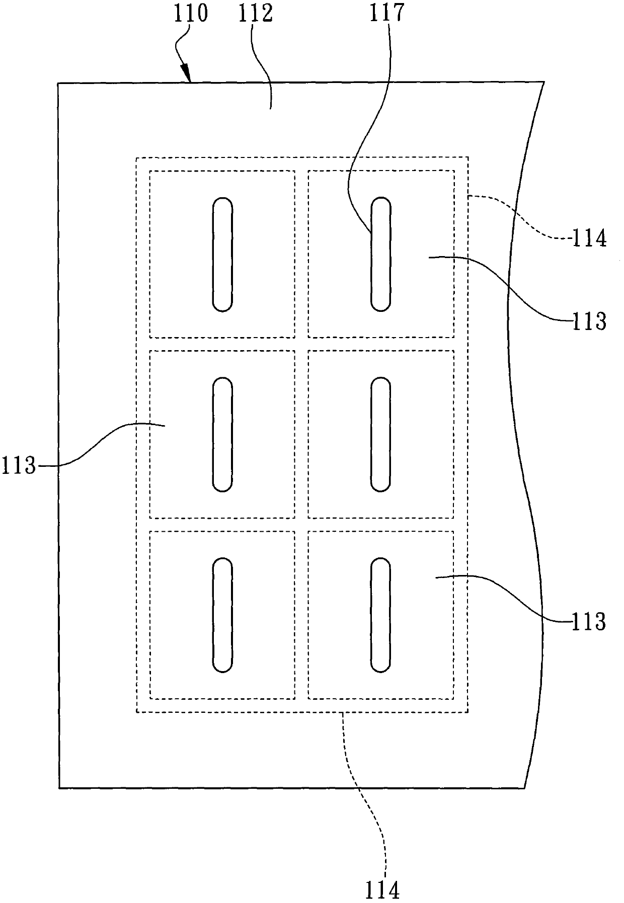
[0035] First, see Figure 4A and Figure 5 As shown, a substrate bar 210 is provided, which has more than four substrate units 212, which are integral connection parts inside the substrate bar 210 during the process and are reserved substrate parts in the semiconductor package structure after the process is manufactured, for Carrying and electrically connecting the chip. The substrate units 212 are arranged in a matrix 211 of N times M. Such as Figure 5 As shown, N is 2, M is 3, and a plurality of substrate units form a 2×3 matrix...
no. 2 Embodiment
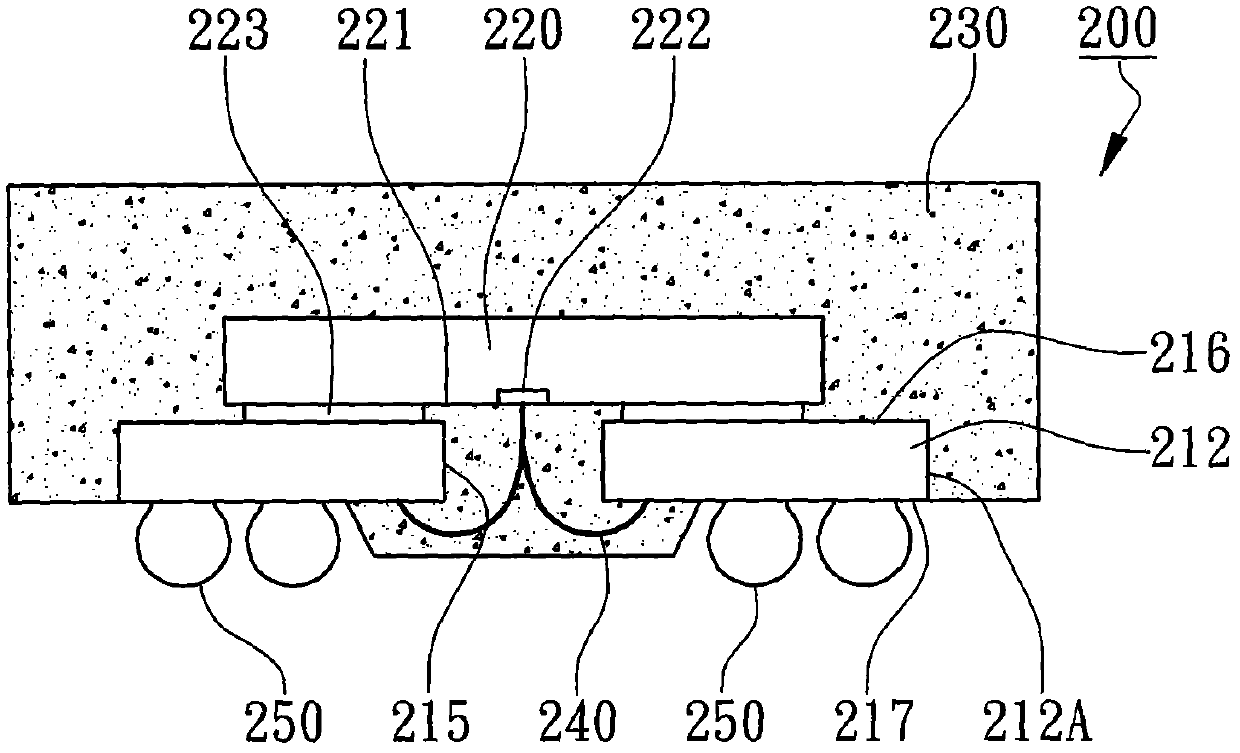
[0042] According to the second embodiment of the present invention, another molding array processing method for covering the side of the substrate is exemplified in Figure 6A to Figure 6H The cross-sectional schematic diagrams of components in each step are used to illustrate that the present invention is applicable to different packaging types, wherein the main components that are the same as those in the first embodiment are marked with the same symbols and will not be described in detail.
[0043] see Figure 6A As shown, a substrate strip 210 is provided having more than four substrate units 212 arranged in an N by M matrix 211 . In this embodiment, in addition to the internal circuit structure, the substrate strip 210 may have more than two internal leads 319 exposed in the central slots 215 of the substrate units 212 . These inner leads 319 can be the extensions of the inner metal circuit layer of the substrate strip 210 or additional suspended inner leads (leads) from...
no. 3 Embodiment
[0049] According to the third embodiment of the present invention, another molding array processing method for covering the side of the substrate is exemplified in Figure 7A to Figure 7G The cross-sectional schematic diagrams of components in each step are used to illustrate that the pre-cut holes need not be formed in the step of providing substrate strips, and the main components that are the same as those in the first embodiment are marked with the same symbols and will not be described in detail.
[0050] see Figure 7A As shown, a substrate strip 210 is provided having more than four substrate units 212 arranged in an N by M matrix 211 . see Figure 7B As shown, more than two chips 220 are disposed on the substrate units 212 , and these chips 220 are electrically connected to the substrate units 212 . see Figure 7C As shown, a dicing tape 470 can be pasted on the lower surface 217 of the substrate strip 210 to carry the substrate strip 210 and be used for subsequent ...
PUM
 Abstract
Description
Claims
Application Information
 - R&D
- Intellectual Property
- Life Sciences
- Materials
- Tech Scout
- Unparalleled Data Quality
- Higher Quality Content
- 60% Fewer Hallucinations
Browse by: Latest US Patents, China's latest patents, Technical Efficacy Thesaurus, Application Domain, Technology Topic, Popular Technical Reports.
© 2025 PatSnap. All rights reserved.Legal|Privacy policy|Modern Slavery Act Transparency Statement|Sitemap|About US| Contact US: help@patsnap.com