

Photoelectric conversion element
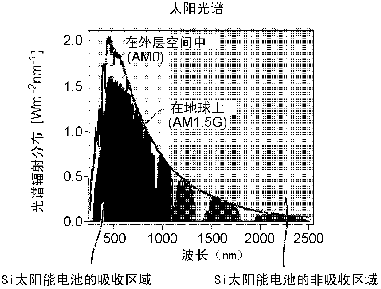
A technology for photoelectric conversion elements and photoelectric conversion layers, which is applied in electrical components, photovoltaic power generation, circuits, etc., and can solve problems such as insufficient absorption of the solar spectrum.
- Summary
- Abstract
- Description
- Claims
- Application Information
AI Technical Summary
Problems solved by technology
Method used
Image

Examples
example 1
[0138] Example 1 (single crystal silicon, S, Ag, nano-mesh electrode)
[0139] will refer to Figures 14A-16D A method of manufacturing the photoelectric conversion element according to Example 1 is described. Figures 14A-16D is a cross-sectional view showing the manufacturing steps of the photoelectric conversion element according to the embodiment.
[0140] Such as Figure 14A As shown, the p-type silicon single crystal substrate 30 was prepared to have a thickness of 500 microns and 1×10 16 Cubic centimeter doping concentration of the substrate. A silicon dioxide film 31 having a thickness of 150 nm is formed on a p-type silicon single crystal substrate 30 by thermal oxidation.
[0141] Such as Figure 14B As shown, after a resist (THMR IP3250, TOKYO OHKA KOGYO Co., Ltd.) solution was coated on the silicon dioxide film 31 by spin coating at 2000 rpm for 30 seconds, the coated resist was heated The plate was heated at 110°C for 90 seconds to evaporate the solvent. Th...
example 2
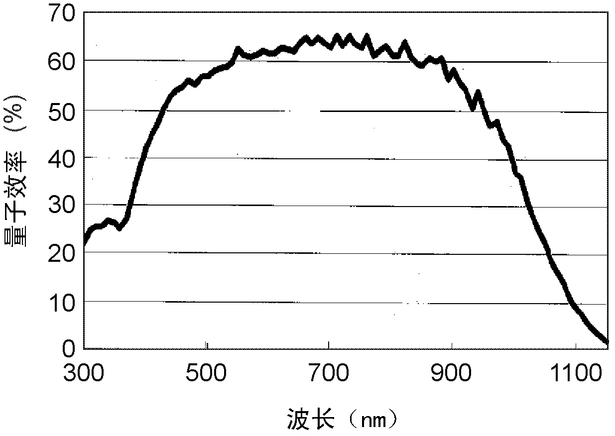
[0159]The results show that the S-doped long-wavelength absorbing layer 33 and the nano-mesh electrode 38 realize an increase in photoelectric conversion efficiency in the long-wavelength region of light due to light absorption in the long-wavelength region of light. Example 2 (single crystal silicon, S, Au, nano-mesh electrodes)
[0160] will refer to Figures 17A-19D A method of manufacturing the photoelectric conversion element according to Example 2 is described. Figures 17A-19D is a cross-sectional view showing the manufacturing steps of the photoelectric conversion element according to Example 2.
[0161] Such as Figure 17A As shown, the preparation has a thickness of 500 µm and a 1 x 10 16 cm -3 A p-type silicon single crystal substrate 30 with a doping concentration of 1000000000000000000000000000000000000000000000000000000. The surface of p-type silicon single crystal substrate 30 is thermally oxidized to form silicon dioxide film 31 having a thickness of 150 n...
example 3
[0180] The results show that the S-doped long-wavelength absorbing layer 33 and the nano-mesh electrode 38 realize an increase in photoelectric conversion efficiency in the long-wavelength region of light due to light absorption in the long-wavelength region of light. Example 3 (single crystal silicon, S-O, Cu, nano-mesh electrodes)
[0181] will refer to Figures 20A-22D A method of manufacturing the photoelectric conversion element according to Example 3 is described. Figures 20A-22D is a sectional view showing a manufacturing step of the photoelectric conversion element according to Example 3.
[0182] Such as Figure 20A As shown, the preparation has a thickness of 500 µm and a 1 x 10 16 cm -3 A p-type silicon single crystal substrate 30 with a doping concentration of 1000000000000000000000000000000000000000000000000000000. The surface of p-type silicon single crystal substrate 30 is thermally oxidized to form silicon dioxide film 31 having a thickness of 150 nm.
...
PUM
| Property | Measurement | Unit |
|---|---|---|
| Mean interval | aaaaa | aaaaa |
| Thickness | aaaaa | aaaaa |
| Thickness | aaaaa | aaaaa |
Abstract
Description
Claims
Application Information