Preparation method of structured grapheme on SiC substrate based on Ni membrane annealing

A structured and graphene technology, applied in the field of microelectronics, can solve the problems of complex process, high production cost, high energy consumption, etc., and achieve the effects of simple process, low porosity and high safety

Inactive Publication Date: 2012-10-10
XIDIAN UNIV
View PDF3 Cites 5 Cited by
  • Summary
  • Abstract
  • Description
  • Claims
  • Application Information

AI Technical Summary

Problems solved by technology

The main disadvantages of this method are: complex process, special removal

Method used


Image

  • Preparation method of structured grapheme on SiC substrate based on Ni membrane annealing
  • Preparation method of structured grapheme on SiC substrate based on Ni membrane annealing

Examples


Embodiment 1

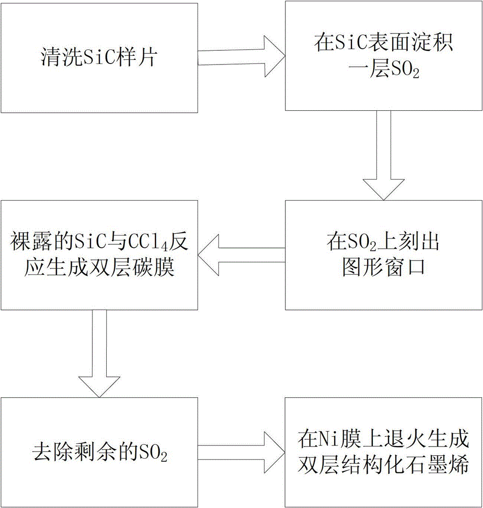
[0025] Step 1: Wash the 6H-SiC sample to remove surface contamination.

[0026] (1.1) Use NH for 6H-SiC substrate 4 OH+H 2 o 2 Soak the sample in the reagent for 10 minutes, take it out and dry it to remove the organic residue on the surface of the sample;

[0027] (1.2) Use HCl+H on the 6H-SiC sample after removing the surface organic residues 2 o 2 The reagent soaked the sample for 10 minutes, took it out and dried it to remove ionic contamination.

[0028] Step 2: Deposit a layer of SiO on the surface of the 6H-SiC sample 2 .

[0029] (2.1) Put the cleaned 6H-SiC sample into the plasma-enhanced chemical vapor deposition PECVD equipment system, adjust the internal pressure of the system to 3.0Pa, adjust the radio frequency power to 100W, and adjust the temperature to 150°C;

[0030] (2.2) Introduce SiH with flow rates of 30sccm, 60sccm and 200sccm into the PECVD system 4 , N 2 O and N 2 , for 20min, making SiH 4 and N 2 O reacts to deposit a layer of SiO with a t...

Embodiment 2

[0051] Step 1: Clean the 4H-SiC sample to remove surface pollutants.

[0052] For 4H-SiC substrates, use NH first 4 OH+H 2 o 2 Soak the sample in the reagent for 10 minutes, take it out and dry it to remove the organic residue on the surface of the sample; then use HCl+H 2 o 2 The reagent soaked the sample for 10 minutes, took it out and dried it to remove ionic contamination.

[0053] Step 2: Deposit a layer of SiO on the surface of the 4H-SiC sample 2 .

[0054] Put the cleaned 4H-SiC sample into the plasma-enhanced chemical vapor deposition PECVD system, adjust the internal pressure of the system to 3.0Pa, adjust the radio frequency power to 100W, and adjust the temperature to 150°C; the flow rate into the system is respectively 30sccm , 60sccm and 200sccm SiH 4 , N 2 O and N 2 , for 75min, making SiH 4 and N 2 O reacts to deposit a layer of SiO with a thickness of 0.8 μm on the surface of the 4H-SiC sample. 2 .

[0055] Step 3: On SiO 2 Spin-coat a layer of p...

Embodiment 3

[0066] Step A: Clean the surface of the 6H-SiC substrate, that is, use NH 4 OH+H 2 o 2 Soak the sample in the reagent for 10 minutes, take it out and dry it to remove the organic residue on the surface of the sample; then use HCl+H 2 o 2 The reagent soaked the sample for 10 minutes, took it out and dried it to remove ionic contamination.

[0067] Step B: Put the cleaned 6H-SiC sample into the PECVD system, adjust the internal pressure of the system to 3.0Pa, adjust the radio frequency power to 100W, and adjust the temperature to 150°C; the flow rates into the system are respectively 30sccm, 60sccm and 200 sccm of SiH 4 , N 2 O and N 2 , for 100min, making SiH 4 and N 2 O reacts to deposit a layer of SiO with a thickness of 1.2 μm on the surface of the 6H-SiC sample. 2 .

[0068] Step C: Same as Step 3 of Example 1.

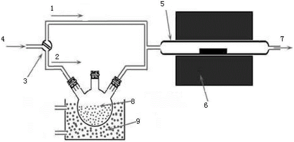
[0069] Step D: Place the windowed sample in the quartz tube 5, and place the quartz tube in the resistance furnace 6; then put the CCl 4 Liquid is pac...


PUM


Abstract

The invention discloses a preparation method of structured grapheme on a SiC substrate based on Ni membrane annealing, which solves the problems of unsmooth surface, poor continuity and uniform layer numbers of the prepared grapheme in the prior art. The preparation method comprises the following steps: performing standard cleaning on a SiC sample, depositing a layer of SiO2 on the surface of the SiC sample, etching a figure window on SiC2; placing the windowed sample in a quartz tube, reacting with bare SiC through gaseous state CC14 under the temperature of 750-1150 DEG C to generate a double layer carbon film; then placing the generated double layer carbon film sample in a buffer hydrofluoric acid solution to remove residual SiO2; performing electron beam deposition of a Ni membrane with thickness of 350-600nm on the other Si samples, placing the sample without SiO2 on the Ni membrane, placing in Ar gas and annealing for 10-20 minutes, and generating the double layer structured grapheme at a window position. The method provided by the invention has the advantages of simple process, high security, smooth surface of the double layer structured grapheme, good continuity and low porosity, and can be used for making a microelectronic electronic device.

Description

technical field [0001] The invention belongs to the technical field of microelectronics, and relates to a semiconductor film material and a preparation method thereof, in particular to a method for preparing structured graphene on a SiC substrate based on Ni film annealing. technical background [0002] Graphene appeared in the laboratory in 2004. At that time, two scientists, Andre Gem and Kostya Novoselov, from the University of Manchester in the United Kingdom discovered that they could obtain more and more graphene in a very simple way. thinner and thinner graphite flakes. They peeled off the graphite flakes from the graphite, then glued the two sides of the flakes to a special adhesive tape, and when the tape was torn off, the graphite flakes could be split in two. Repeatedly doing this, the flakes got thinner and thinner, and eventually, they got a flake made of just one layer of carbon atoms, which is graphene. Since then, new methods of preparing graphene have emer...

Claims


Application Information

Patent Timeline
IPC IPC(8): C01B31/04C01B32/186
Inventor 郭辉张克基张玉明张凤祁雷天民邓鹏飞
Owner XIDIAN UNIV
Why Eureka
Try Eureka