Inversion high voltage alternating/direct current light-emitting diode and manufacture method thereof

A technology for light-emitting diodes and a manufacturing method, which is applied to electrical components, circuits, semiconductor devices, etc., can solve the problems of light output efficiency and heat dissipation performance to be improved, and achieve the effect of facilitating layout design and reducing shading

Inactive Publication Date: 2012-10-10
钟伟荣
View PDF4 Cites 15 Cited by
  • Summary
  • Abstract
  • Description
  • Claims
  • Application Information

AI Technical Summary

Problems solved by technology

However, the light extraction efficiency and heat dissipation performance of this high-voltage light-emitting diode still need to be improved.

Method used


Image

  • Inversion high voltage alternating/direct current light-emitting diode and manufacture method thereof
  • Inversion high voltage alternating/direct current light-emitting diode and manufacture method thereof
  • Inversion high voltage alternating/direct current light-emitting diode and manufacture method thereof

Examples


no. 1 example

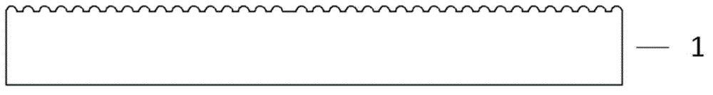
[0045] figure 1 It shows that according to the first embodiment of the present invention, a first rough surface is formed on the front surface of the sapphire substrate 1 by plasma dry etching.

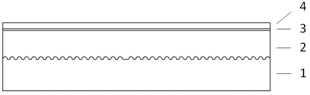
[0046] figure 2 It shows that according to the first embodiment of the present invention, the main N-GaN layer 2 , the light emitting layer 3 and the P-GaN layer 4 are sequentially grown from the front side of the roughened sapphire substrate 1 outward.

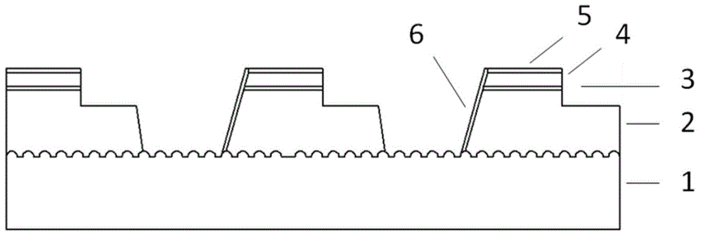
[0047] image 3It shows that according to the first embodiment of the present invention, several independent light-emitting units are formed on the chip by using well-known semiconductor technology, and a current diffusion layer 5 is evaporated on the P-GaN layer 4 to form an ohmic contact, and each light-emitting unit The side wall forms a PN junction insulating layer 6; the current spreading layer 5 can be a metal such as nickel, silver, platinum, gold, and an alloy of the above metals, or an oxide metal such as indium tin oxide...


PUM

PropertyMeasurementUnit
thicknessaaaaaaaaaa
thicknessaaaaaaaaaa

Abstract

The invention provides an inversion high voltage alternating / direct current light-emitting diode and a manufacture method thereof. The light-emitting diode comprises a routing electrode, a sapphire substrate, an N-GaN layer, a light-emitting layer, a P-gAn layer, a current diffusion layer, an insulating layer, a metal reflecting layer, an insulation flat layer, a bonding metal medium layer and a support substrate from top to bottom. Mat surfaces formed by plasma dry etching are arranged on two sides of the sapphire substrate, a through hole formed by laser drilling is arranged in the sapphire substrate, and metal is filled in the through hole to enable an electrode on the N-GaN layer and the routing electrode to be connected. The light-emitting diode enables a wafer to be inversely bonded on a substrate of a radiating support, a positive electrode and a negative electrode are respectively located on the upper side and the lower side of a chip, each light-emitting unit on the chip forms an inversed trapezoidal structure due to inversion, each light-emitting unit is wrapped by the reflecting layer to form a structure with an upward opening and effects of reflecting cups, simultaneously shielding of electrodes on light-emitting directions is reduced, only the negative electrode is arranged above the chip, and layout design of the light-emitting units of the high voltage light-emitting diode can be convenient.

Description

technical field [0001] The invention relates to light-emitting diode technology, in particular to a flip-chip high-voltage AC / DC light-emitting diode and a manufacturing method thereof. Background technique [0002] For the design of high-power LEDs, most major manufacturers currently focus on large-size single low-voltage DC LEDs. There are two methods, one is the traditional horizontal structure, and the other is the vertical conductive structure. As far as the first method is concerned, its manufacturing process is almost the same as that of ordinary small-sized dies. In other words, the cross-sectional structure of the two is the same, but different from small-sized dies, high-power LEDs often need to operate at high currents Under the circumstances, a little bit of unbalanced P and N electrode design will lead to serious current crowding effect (Current crowding). As a result, in addition to making the LED chip fail to achieve the brightness required by the design, it w...

Claims


Application Information

Patent Timeline
Patent Type & Authority Applications(China)
IPC IPC(8): H01L33/20H01L33/14H01L33/10H01L33/00
Inventor 钟伟荣熊威李政宪
Owner 钟伟荣
Why Eureka
Try Eureka