Low-cost efficient solar cell electrode grid line structure

A technology for solar cells and electrode grid lines, applied in circuits, electrical components, semiconductor devices, etc., can solve the problems of rising paste costs, increased grid line shielding area, high square resistance and low contact resistance, etc., and achieve silver paste consumption Reduce, improve conversion efficiency, reduce the effect of contact surface recombination

Inactive Publication Date: 2012-10-17
JA SOLAR TECH YANGZHOU
View PDF5 Cites 31 Cited by
  • Summary
  • Abstract
  • Description
  • Claims
  • Application Information

AI Technical Summary

Problems solved by technology

[0003] From the perspective of the electrode grid structure design of crystalline silicon solar cells, it is difficult to obtain lower contact resistance on the surface of high sheet resistance by traditional screen printing technology. To improve the conversion efficiency of the cell, it is necessary to increase the area of ​​the metal grid to reduce the series Resistance, but this will increase the shielding area of ​​the gate line, and also increase the paste cost

Method used


Image

  • Low-cost efficient solar cell electrode grid line structure
  • Low-cost efficient solar cell electrode grid line structure
  • Low-cost efficient solar cell electrode grid line structure

Examples


Embodiment 1

[0019] For 156x156 size polysilicon cells, the design of electrode grid line structure is as follows (such as Figure 3-4 shown):

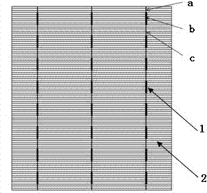
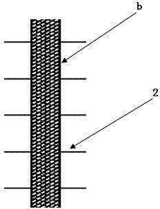
[0020] 1) The number of busbar lines is 3, which are distributed symmetrically around the center of the silicon wafer. The distance between the three busbar lines is 52mm; the busbar lines are divided into 8 sections, which are connected alternately with thin lines. The width of the busbar is 1.4mm and the length is 10mm; the width of the thin line part a at both ends of the busbar is 0.3mm and the length is 5mm; the width of the thin line part c connecting each segment in the middle of the busbar is 0.3mm and the length is 9mm; Segment b adopts a rectangular hollow design, distributed in an array, with a pitch of 0.1mm and an offset angle of 30°.

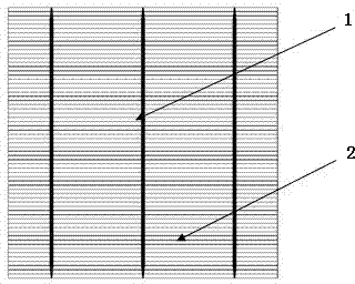
[0021] 2) Thin grid lines 2 are distributed in parallel with equal distances perpendicular to the main grid lines, the number of thin grid lines is 90, the width of the thin grid lines is 0.05mm, and ...

Embodiment 2

[0023] For a 125x125 size monocrystalline silicon cell, the electrode grid structure is designed as follows:

[0024] 1) The number of main grid lines is 2, which are distributed symmetrically around the center of the silicon wafer. The main grid lines are divided into 6 sections, which are connected alternately with thin lines. The length of the two main grid line segments on both sides is 13.4 mm, the length of the segmented part of the central busbar line is 8mm, the width of the segmented part of the busbar line is 1.4mm, the width of the thin lines at both ends of the busbar line is 0.3mm, and the length is 5mm, and the middle part of the busbar line connects each segment The width of the thin line part is 0.3mm, and the length is 10.8mm. The segmented part adopts a rectangular hollow design, distributed in an array, with a pitch of 0.1mm and an offset angle of 30°.

[0025] 2) The thin grid lines are distributed equidistantly perpendicular to the main grid, the number of...

Embodiment 3

[0027] For a 156x156 size monocrystalline silicon cell, the electrode grid structure is designed as follows:

[0028] 1) The number of busbar lines is 3, which are distributed symmetrically around the center of the silicon wafer. The distance between the three busbar lines is 52mm. The busbar lines are divided into 8 sections, which are alternately connected by thin lines. The width is 1.4mm and the length is 8mm; the width a of the thin lines at both ends of the busbar is 0.3mm and the length is 5mm; Adopt rectangular hollow design, array distribution, pitch 0.1mm, offset angle 30°.

[0029] 2) Thin grid lines 2 are distributed parallel to the vertical main grid lines at equal intervals, the number of thin grid lines is 90, the width of the thin grid lines is 0.05mm, and the distance between the grid lines is 1.54mm.


PUM


Abstract

The invention discloses a low-cost efficient solar cell electrode grid line structure which comprises two parts of main grid lines and thin grid lines, wherein the main grid lines are symmetrically distributed by taking a silicon wafer center as a center, the thin grid lines are equidistantly distributed in the way of being vertical to the main grid lines in parallel, the main grid lines adopt a sectional type design, and all the subsections are connected by thin lines. The electrode grid line structure adopts a design that the grid lines are thinned, the shading areas of the grid lines are reduced, the number of the grid lines is increased so that the lateral transmission loss of a carrier is lowered and the collection efficiency of the carrier is increased; moreover, the main grid lines are divided into sections, thinned and hollowed out additionally, so the silver usage is reduced, the manufacturing cost of a solar cell is reduced, meanwhile, the contact area compound is lowered, accordingly, the open-circuit voltage of the solar cell is increased, and the cost is greatly lowered; and compared with the widespread products of the industry, in the design scheme which is obtained by optimizing the scheme, the shading area of the grid lines on the front side of the solar cell is reduced by about 1%, the conversion efficiency is improved by 0.2-0.3%, and the silver paste consumption is reduced by about 35%.

Description

technical field [0001] The invention relates to the field of solar cell manufacturing technology, in particular to an electrode grid line structure of a solar cell. Background technique [0002] As solar energy becomes an increasingly viable clean energy, in order to improve its market competitiveness, continuously improving the conversion efficiency of solar cells and reducing manufacturing costs have become the focus of the solar cell industry. However, most of the various types of high-efficiency batteries currently developed require the addition of new equipment and new processes, which increases production costs, and the technical threshold is high, making it difficult to achieve mass production. Therefore, research on how to improve battery efficiency and reduce production costs on the basis of existing processes has become the best way at this stage. [0003] From the perspective of the electrode grid structure design of crystalline silicon solar cells, it is difficu...

Claims


Application Information

Patent Timeline
Patent Type & Authority Applications(China)
IPC IPC(8): H01L31/0224
Inventor 李积伟赵永乐万祥刘源宋锋兵曾云杨虎王芹芹
Owner JA SOLAR TECH YANGZHOU
Why Eureka
Try Eureka