Semiconductor element and manufacturing method thereof

A manufacturing method and semiconductor technology, applied in semiconductor/solid-state device manufacturing, semiconductor devices, electrical components, etc., can solve problems such as the influence of source and drain characteristics, and achieve the effect of good component characteristics

Inactive Publication Date: 2012-10-24
AU OPTRONICS CORP
View PDF4 Cites 2 Cited by
  • Summary
  • Abstract
  • Description
  • Claims
  • Application Information

AI Technical Summary

Problems solved by technology

However, the current etching gas used to form the contact window usually contains components such as oxygen, sulfur, fluorine or chlorine that may oxidize silver, resulting in the characteristics of the source and drain being affected

Method used


Image

  • Semiconductor element and manufacturing method thereof
  • Semiconductor element and manufacturing method thereof
  • Semiconductor element and manufacturing method thereof

Examples


Embodiment Construction

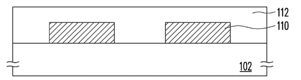
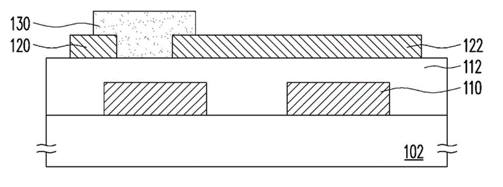
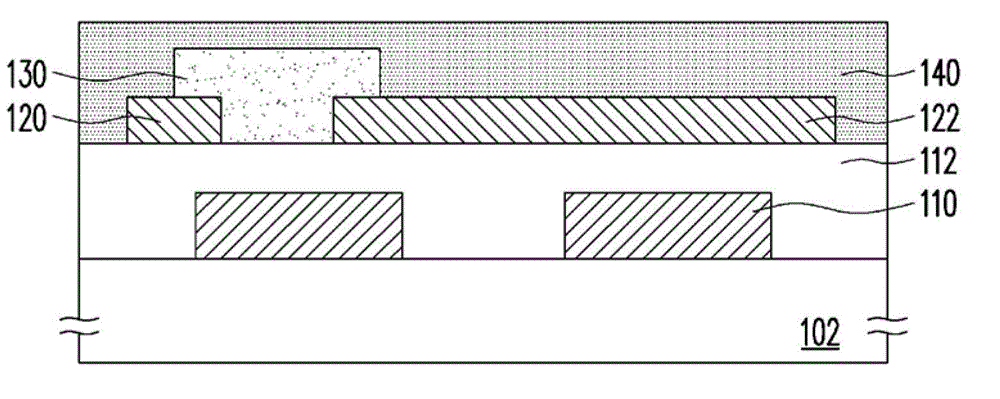
[0026] Figure 1A to Figure 1H is a schematic cross-sectional flow diagram of a method for manufacturing a semiconductor device according to an embodiment of the present invention. Please refer to Figure 1A , firstly, the gate 110 is formed on the substrate 102 . In this embodiment, the substrate 102 is, for example, a hard substrate such as a glass substrate, a quartz substrate, or a silicon wafer, or a flexible substrate such as a plastic substrate or a metal film. The gate 110 is, for example, a single-layer or multi-layer stacked conductive material, and the conductive material can be selected from copper (Cu), molybdenum (Mo), titanium (Ti), aluminum (Al), tungsten (W), silver (Ag), At least one member of the group consisting of gold (Au) and alloys thereof. The gate 110 can be fabricated by forming a conductive layer and performing photolithography and etching processes on the conductive layer to pattern the conductive layer. The method of forming the conductor layer...


PUM


Abstract

The present invention discloses a semiconductor element and a manufacturing method thereof. The manufacturing method comprises the steps of: forming a grid electrode on a substrate; forming a source electrode and a drain electrode above or below the grid electrode; forming a first insulating layer for covering the source electrode and the drain electrode; forming a semiconductor layer between the source electrode and the drain electrode; patterning the first insulating layer for at least covering the drain electrode; forming a second insulating layer on the patterned first insulating layer; etching the second insulating layer to form a second opening which exposes the patterned first insulating layer and is arranged above the drain electrode, wherein, an etching selection ratio, i.e., the second insulating layer / the patterned first insulating layer, is greater than 1; performing wet etching for the patterned first insulating layer via the second opening, so as to form a first opening which is communicated with the second opening and exposes the drain electrode; and forming a pixel electrode which is electrically connected with the drain electrode via the first opening and the second opening.

Description

technical field [0001] The present invention relates to an element and its manufacturing method, and in particular to a semiconductor element and its manufacturing method. Background technique [0002] Due to the advantages and characteristics of organic thin-film transistor (OTFT), such as thinness, flexibility, and low manufacturing process temperature, it has been widely used in liquid crystal displays, organic light-emitting displays, electrophoretic displays and other devices. . [0003] In organic thin film transistor manufacturing technology, in order to take into account good charge injection capability and cost considerations, the source and drain are usually made of silver, and the exposed source and drain are formed in the protective layer covering the source and drain. contact window. However, the current etching gas used to form the contact window usually contains components such as oxygen, sulfur, fluorine or chlorine that may oxidize silver, resulting in the...

Claims


Application Information

Patent Timeline
IPC IPC(8): H01L51/52H01L51/50H01L51/56
Inventor 梁育馨林暐翔朱书纬萧祥志刘景洋刘思呈黄志杰
Owner AU OPTRONICS CORP
Why Eureka
Try Eureka