Light-emitting device, electronic device, and lighting device utilizing phosphorescence
一种发光装置、磷光的技术,应用在照明装置、电致发光光源、发光材料等方向
- Summary
- Abstract
- Description
- Claims
- Application Information
AI Technical Summary
Problems solved by technology
Method used
Image
Examples
Embodiment approach 1
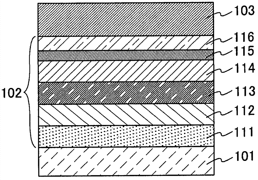
[0095] In this embodiment, as a light-emitting element that can be applied to a light-emitting device that emits light using phosphorescence, refer to figure 1 A light-emitting device using a phosphorescent organometallic iridium complex for a light-emitting layer will be described.
[0096] In the light-emitting element shown in this embodiment mode, as figure 1 As shown, an EL layer 102 including a light emitting layer 113 is sandwiched between a pair of electrodes (a first electrode (anode) 101 and a second electrode (cathode) 103). The hole injection layer 111, the hole transport layer 112, the electron transport layer 114, the electron injection layer 115, the charge generation layer (E) 116, etc. are formed.
[0097] By applying a voltage to this light-emitting element, holes injected from the first electrode 101 side and electrons injected from the second electrode 103 side recombine in the light-emitting layer 113 to bring the phosphorescent organometallic iridium com...
Embodiment approach 2
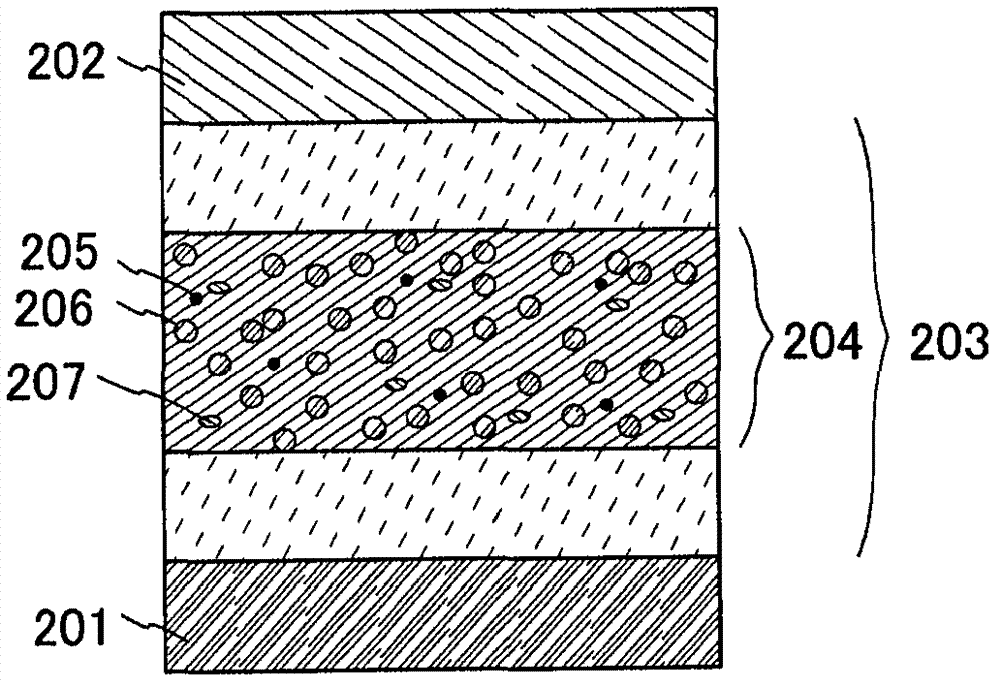
[0151] In this embodiment mode, a light-emitting device in which two or more other organic compounds are used for the light-emitting layer in addition to the phosphorescent organometallic iridium complex will be described as one aspect of the present invention.
[0152] The light-emitting element shown in this embodiment mode has figure 2 As shown, the structure includes the EL layer 203 between a pair of electrodes (the anode 201 and the cathode 202). In addition, the EL layer 203 has at least the light-emitting layer 204, and the EL layer 203 may further include a hole injection layer, a hole transport layer, an electron transport layer, an electron injection layer, a charge generation layer (E), and the like. In addition, as the hole injection layer, hole transport layer, electron transport layer, electron injection layer, and charge generation layer (E), those described in Embodiment Mode 1 can be used.
[0153] The light-emitting layer 204 described in this embodiment m...
Embodiment approach 3
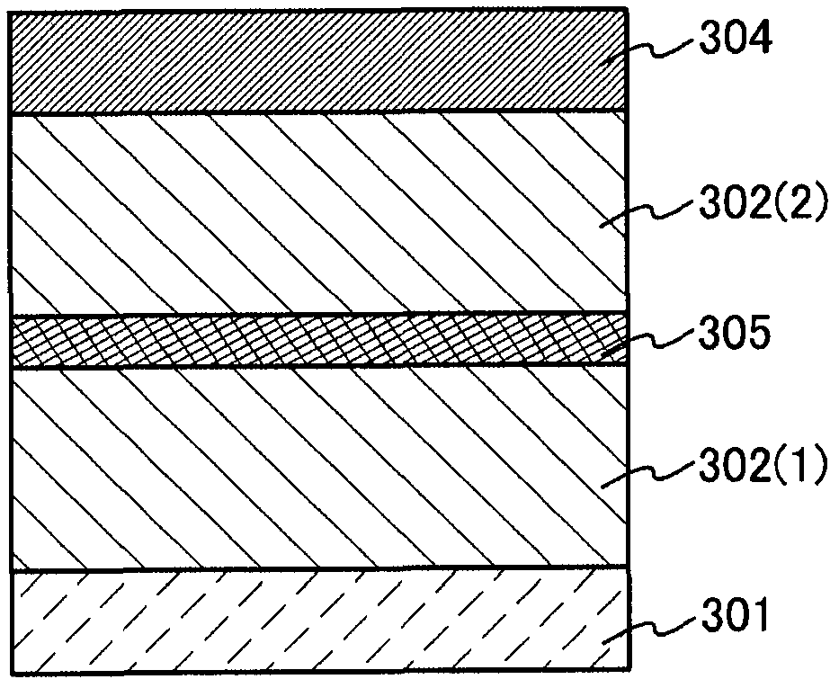
[0170] In this embodiment mode, a light-emitting element having a structure having a plurality of EL layers (hereinafter referred to as a tandem light-emitting element) with a charge generation layer interposed therebetween will be described as one aspect of the present invention.
[0171] The light-emitting element shown in this embodiment is as follows Figure 3A A tandem light emitting element having a plurality of EL layers (first EL layer 302(1) and second EL layer 302(2)) between a pair of electrodes (first electrode 301 and second electrode 304) as shown .
[0172] In the present embodiment, the first electrode 301 is an electrode serving as an anode, and the second electrode 304 is an electrode serving as a cathode. In addition, as the first electrode 301 and the second electrode 304, the same configuration as that of the first embodiment can be employed. In addition, although the plurality of EL layers (the first EL layer 302(1) and the second EL layer 302(2)) may h...
PUM
| Property | Measurement | Unit |
|---|---|---|
| visible light transmittance | aaaaa | aaaaa |
| reflectivity | aaaaa | aaaaa |
| reflectivity | aaaaa | aaaaa |
Abstract
Description
Claims
Application Information


