A kind of epitaxial wafer of light-emitting diode and its manufacturing method

A technology of light-emitting diodes and epitaxial wafers, applied in the field of diodes, can solve the problems of strengthening the polarization of quantum well regions, bending the energy band of quantum well regions, and affecting internal quantum efficiency, so as to improve internal quantum efficiency and increase the probability of electron tunneling , Improve the effect of compounding efficiency

Active Publication Date: 2015-09-23
HC SEMITEK ZHEJIANG CO LTD
View PDF6 Cites 0 Cited by
  • Summary
  • Abstract
  • Description
  • Claims
  • Application Information

AI Technical Summary

Problems solved by technology

[0005] Each quantum barrier layer in the MQW layer of the existing epitaxial wafer is a single-layer structure, and the atoms in each layer are arranged neatly, and lattice mismatch will occur at the junction of the quantum barrier layer and the adjacent quantum well layer; and the lattice mismatch The combination will generate compressive stress, strengthen the polarization of the quantum well region, cause the energy band of the quantum well region to bend, and affect the internal quantum efficiency of the LED.

Method used


Image

  • A kind of epitaxial wafer of light-emitting diode and its manufacturing method
  • A kind of epitaxial wafer of light-emitting diode and its manufacturing method

Examples


Embodiment 1

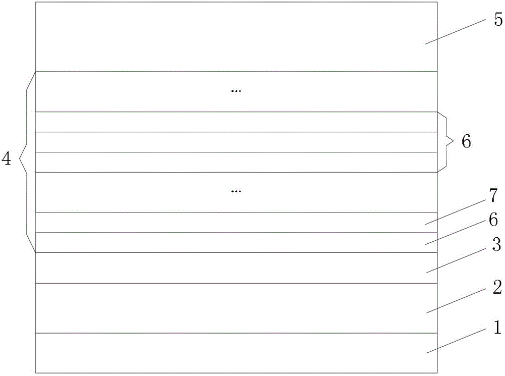
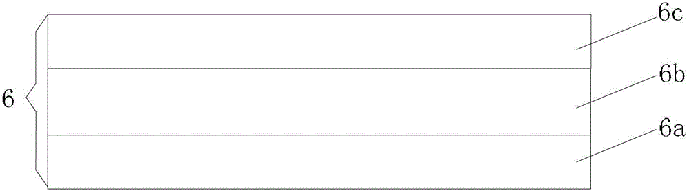
[0021] see figure 1 Embodiment 1 of the present invention provides an epitaxial wafer of a light emitting diode, the epitaxial wafer includes a substrate layer 1, a buffer layer 2 covering the substrate layer 1 in sequence, an N-type layer 3, an MQW layer 4 and a P-type layer 5 The N-type layer 3 is made of n-type doped GaN; the MQW layer 3 includes several quantum barrier layers 6 and several quantum well layers 7 grown alternately with each quantum barrier layer 6 . Wherein, at least one quantum barrier layer 6 in the several quantum barrier layers 6 includes three sub-quantum barrier layers; the sub-quantum barrier layer positioned in the middle of the three sub-quantum barrier layers is made of n-type doped Al x In y Ga 1-x-y N, the n-type doping concentration is not greater than the n-type doping concentration of the N-type layer 3; the other two quantum barrier layers are made of undoped GaN; wherein, 0

[0022] The beneficial effects brought by the tech...

Embodiment 2

[0024] An embodiment of the present invention provides an epitaxial wafer of a light emitting diode. The epitaxial wafer includes a substrate layer 1 , a buffer layer 2 covering the substrate layer 1 in sequence, an N-type layer 3 , an MQW layer 4 and a P-type layer 5 .

[0025] Specifically, the substrate layer 1 is a sapphire substrate.

[0026] Specifically, the buffer layer 2 is a composite layer, including a low-temperature buffer layer and an undoped GaN layer.

[0027] Specifically, the N-type layer 3 is made of n-type doped GaN. Preferably, its n-type doping is obtained by Si doping, and its doping concentration is 5×10 18 cm -3 .

[0028] Wherein, the MQW layer 3 includes several quantum barrier layers 6 and several quantum well layers 7 grown alternately with each quantum barrier layer 6 . And, at least one quantum barrier layer 6 in all quantum barrier layers 6 comprises three sub-quantum barrier layers; x In y Ga 1-x-y N, the n-type doping concentration is n...

Embodiment 3

[0038] Embodiment 3 of the present invention provides a method for manufacturing an epitaxial wafer of a light-emitting diode. The method includes providing a substrate and sequentially growing a buffer layer, an N-type layer, several quantum barrier layers in the MQW layer, and several Each quantum barrier layer alternates quantum well layers and P-type layers. Wherein, growing at least one quantum barrier layer in the several quantum barrier layers includes:

[0039] growing the quantum barrier layer to a first thickness using undoped GaN;

[0040] n-doped Al x In y Ga 1-x-y N is deposited at a predetermined doping concentration to grow the quantum barrier layer to a second thickness;

[0041] growing the quantum barrier layer to a third thickness using undoped GaN;

[0042] Wherein, the predetermined doping concentration is not greater than the doping concentration of the N-type layer; 0

[0043] Further, the second thickness is 0-10 nm; the first thicknes...


PUM


Abstract

The invention discloses an epitaxial wafer of a light-emitting diode (LED) and the manufacturing method of the epitaxial wafer and belongs to the technical field of diodes. The epitaxial wafer comprises a substrate layer, a buffer layer, an N-type layer, a multiple quantum well (MQW) layer and a P-type layer, wherein the substrate layer, the buffer layer, the N-type layer, the MQW layer and the P-type layer are sequentially covered on the substrate layer; the N-type layer is made of n-type doped GaN; the MQW layer comprises a plurality of quantum barrier layers and a plurality of quantum well layers which alternately grow with the quantum barrier layers; at least one of the quantum barrier layers comprises three sub-quantum barrier layers; a sub-quantum barrier layer positioned in the middle of the three sub-quantum barrier layers is made of n-type doped AlxInyGa[1-x-y]N, and the n-type doping concentration of the sub-quantum barrier layer is not greater than that of the N-type layer; and the other two sub-quantum barrier layers are made of non-doped GaN, wherein x is more than 0 and less than 1, and y is more than 0 and less than 1. According to the technical scheme, the electrostatic resistance of the LED can be improved.

Description

technical field [0001] The invention relates to the technical field of diodes, in particular to an epitaxial wafer of a light emitting diode and a manufacturing method thereof. Background technique [0002] LED (Light Emitting Diode, light-emitting diode) chip is a semiconductor wafer, which is the core component of LED. The LED chip includes a GaN-based epitaxial wafer grown on a substrate, and electrodes fabricated on the epitaxial wafer. [0003] Among them, the epitaxial wafer mainly includes an N-type layer, an MQW (Multiple Quantum Well, multiple quantum well) layer and a P-type layer. When the current passes through the epitaxial wafer, the electrons in the N-type layer and the holes in the P-type layer recombine in the MQW layer, and then emit energy in the form of photons. Therefore, the MQW layer is also called the light emitting layer. The MQW layer is a multilayer structure formed by the alternate growth of thin layers of two different semiconductor materials....

Claims


Application Information

Patent Timeline
Patent Type & Authority Patents(China)
IPC IPC(8): H01L33/06H01L33/32H01L33/00
Inventor 王明军魏世祯胡加辉
Owner HC SEMITEK ZHEJIANG CO LTD
Why Eureka
Try Eureka