Polishing method and gate forming method

A grid, polishing liquid technology, applied in surface polishing machine tools, grinding/polishing equipment, electrical components, etc., can solve the problems of product yield reduction, device scrapping, etc., and achieve the effect of improving yield

Active Publication Date: 2015-07-08
SEMICON MFG INT (SHANGHAI) CORP
View PDF4 Cites 0 Cited by
  • Summary
  • Abstract
  • Description
  • Claims
  • Application Information

AI Technical Summary

Problems solved by technology

The residual metal layer will cause the device to be scrapped, and the yield rate of the product will be greatly reduced

Method used


Image

  • Polishing method and gate forming method
  • Polishing method and gate forming method
  • Polishing method and gate forming method

Examples


Embodiment Construction

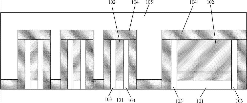
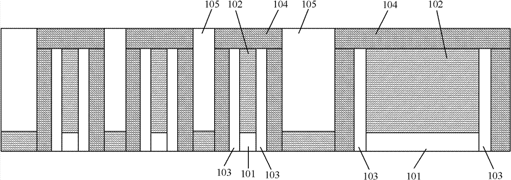
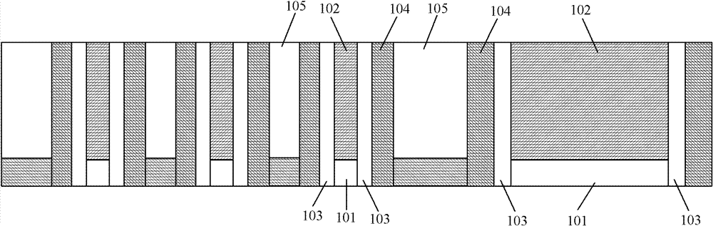
[0049] In the prior art, after the first-stage polishing operation is performed on the metal layer covering the dielectric layer until the dielectric layer is exposed, problems of scratching of the dielectric layer and residual metal layer occur. In this technical solution, the second-stage polishing operation is performed on the metal layer and the dielectric layer by using a non-selective polishing liquid, so that the scratches on the dielectric layer after the first-stage polishing operation can be repaired, and the The residual metal layer (part of the metal layer to be removed) after the first-stage polishing operation.

[0050] In order to make the above objects, features and advantages of the present invention more comprehensible, specific implementations of the present invention will be described in detail below in conjunction with the accompanying drawings.

[0051]In the following description, specific details are set forth in order to provide a thorough understandin...


PUM

PropertyMeasurementUnit
sizeaaaaaaaaaa
thicknessaaaaaaaaaa

Abstract

The invention discloses a polishing method and a gate forming method. The gate forming method comprises the following steps of: forming a pseudo-gate structure on a semiconductor substrate, wherein the pseudo-gate structure comprises a sacrificial oxide layer and a polysilicon layer which covers the sacrificial oxide layer; forming a side wall on the periphery of the pseudo-gate structure; forming a silicon nitride layer and a dielectric layer which covers the silicon nitride layer, wherein the silicon nitride layer covers the polysilicon layer, the side wall and the substrate; polishing the dielectric layer until the silicon nitride layer is exposed; polishing the silicon nitride layer and stopping polishing at the polysilicon layer; removing the pseudo-gate structure to form an opening; forming a gate dielectric layer and a metal layer which covers the gate dielectric layer in the opening in sequence; performing first-stage polishing operation on the metal layer until the dielectric layer is exposed to form a metal gate and a residual metal layer; and performing second-stage polishing operation on the metal layer, the dielectric layer and the silicon nitride layer by adopting a non-selective polishing solution to remove the residual metal layer.

Description

technical field [0001] The invention relates to the field of semiconductor manufacturing, in particular to a polishing method and a method for forming a grid. Background technique [0002] In the semiconductor manufacturing process, a flat wafer surface is extremely important for the miniaturization and high density of devices. The traditional method of flattening the wafer surface is chemical mechanical polishing (CMP, Chemical Mechanical Polishing). In this method, a polishing liquid is added between the wafer surface and the polishing pad, and the surface of the wafer is planarized by using the mechanical force and the chemical reaction between the polishing liquid and the wafer surface. In particular, when CMP is performed on a metal material, the abrasive is in contact with the metal surface to generate metal oxides, and the metal oxides are removed by grinding to achieve a polishing effect. [0003] With the continuous development of semiconductor manufacturing techno...

Claims


Application Information

Patent Timeline
Patent Type & Authority Patents(China)
IPC IPC(8): H01L21/302B24B29/02H01L21/28
Inventor 蒋莉黎铭琦
Owner SEMICON MFG INT (SHANGHAI) CORP
Why Eureka
Try Eureka