
Transistor and forming method thereof

A transistor and semiconductor technology, applied in semiconductor devices, semiconductor/solid-state device manufacturing, electrical components, etc., can solve problems such as unsolved problems, and achieve the effects of preventing damage, improving performance, and having a small k value.

Active Publication Date: 2012-11-28
SEMICON MFG INT (SHANGHAI) CORP
View PDF5 Cites 3 Cited by
  • Summary
  • Abstract
  • Description
  • Claims
  • Application Information

AI Technical Summary

Problems solved by technology

But it didn't solve the above problem

Method used


Image

  • Transistor and forming method thereof
  • Transistor and forming method thereof
  • Transistor and forming method thereof

Examples


Embodiment Construction

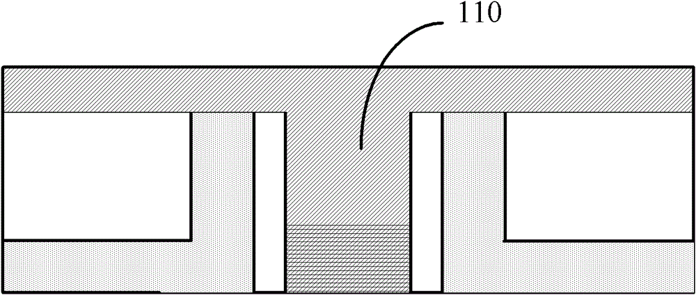
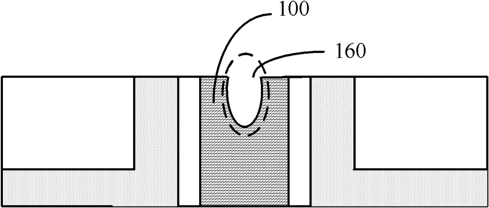
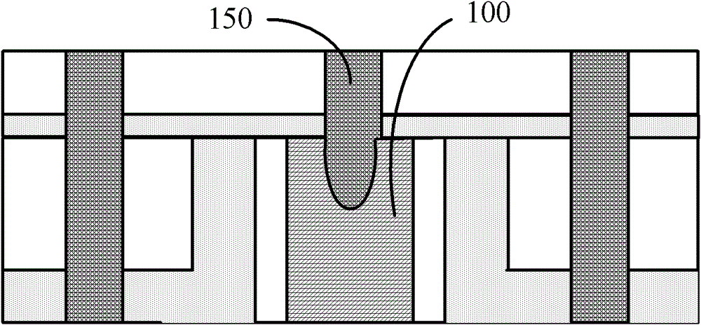
[0032] It can be seen from the background art that the performance of the transistor formed by the existing transistor forming method is not good enough. The inventors conducted research on the above problems and believed that since aluminum is a very soft material, it is easy to cause damage to aluminum during grinding, such as scratches and corrosion on the surface of aluminum. If scratches and corrosion occur in the area of ​​the metal gate, the function and reliability of the formed device can be affected, please refer to figure 1 with figure 2 , during the process of planarizing the metal layer 110 by chemical mechanical polishing to form the metal grid 100, a damage 160 is formed on the surface of the metal grid 100; please refer to image 3 , in the subsequent step of forming the conductive plug 150 , the conductive plug 150 will penetrate into the metal gate 100 . In a more serious situation, in the step of forming an opening in the dielectric layer using an etchin...


PUM

PropertyMeasurementUnit
Thicknessaaaaaaaaaa
Thicknessaaaaaaaaaa

Abstract

The invention discloses a transistor forming method which comprises the following steps: providing a semiconductor substrate, wherein a first medium layer is formed on the surface of the semiconductor substrate, a first opening is formed in the first medium layer and filled with a metal layer, and the metal layer is fully filled in the first opening and covers the first medium layer; flattening the metal layer until the first medium layer is exposed to form a metal grid; forming an etching stop layer and a second medium layer positioned on the surface of the etching stop layer sequentially on the surface of the first medium layer and the surface of the metal grid; forming a second opening penetrating through the second medium layer and the etching stop layer, wherein the second opening is exposed from the metal grid; forming a compensation metal layer on the surface of the exposed metal grid; and forming a conductive plug fully filled in the second opening on the surface of the compensation metal layer. The invention also provides a transistor formed by the method. Through the invention, the performance of the transistor can be improved.

Description

technical field [0001] Embodiments of the present invention relate to the field of semiconductors, in particular to transistors and methods of forming the same. Background technique [0002] With the continuous development of semiconductor manufacturing technology, the feature size (CD, Critical Dimension) of transistors in integrated circuits is getting smaller and smaller. In order to solve a series of problems caused by small-sized devices, high dielectric constant (High-K) The technology of combining gate dielectric layer and metal gate (Metal Gate) has been introduced into the manufacturing process of MOS transistors. At present, high-K metal gate (HKMG, High-K Metal Gate) technology has become the first choice for manufacturing processes below 32nm. mainstream. Among them, chemical mechanical polishing (CMP, Chemical Mechanical Polishing) for the metal gate is one of the most important process steps. The mechanism of CMP is that the surface material reacts chemically...

Claims


Application Information

Patent Timeline
IPC IPC(8): H01L21/336H01L21/28H01L29/78H01L29/49
Inventor 蒋莉黎铭琦
Owner SEMICON MFG INT (SHANGHAI) CORP
Features
  • Generate Ideas
  • Intellectual Property
  • Life Sciences
  • Materials
  • Tech Scout
  • Unparalleled Data Quality
  • Higher Quality Content
  • 60% Fewer Hallucinations
Learn More