Method for manufacturing distributed feedback laser device array by virtue of selection region epitaxy technology
A technology of selective area epitaxy and laser arrays, applied in lasers, laser devices, semiconductor lasers, etc., and can solve problems such as deviation from peak gain, change of quantum well emission wavelength, and change of effective refractive index.
- Summary
- Abstract
- Description
- Claims
- Application Information
AI Technical Summary
Problems solved by technology
Method used
Image
Examples
no. 1 example
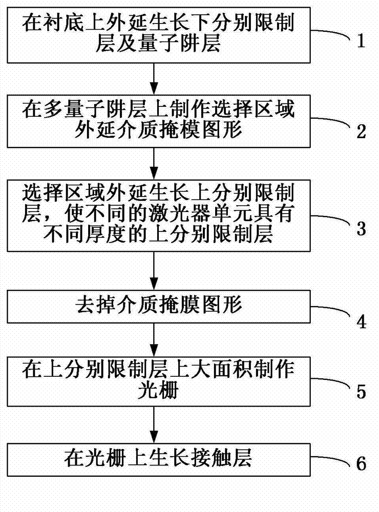
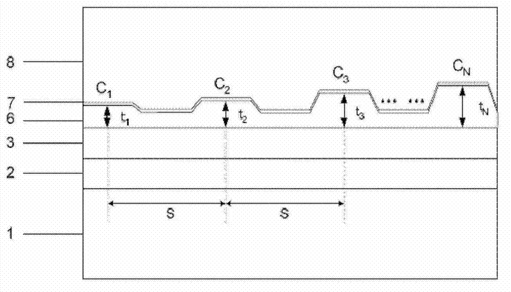
[0031] see figure 1 , image 3 , Figure 5 and Image 6 As shown, the present invention provides a method (first embodiment) for making a distributed feedback laser array using the selective area epitaxy technique, comprising the following steps:
[0032] Step 1: Epitaxially grow the confinement layer 2 and the quantum well layer 3 respectively on the substrate 1. The substrate 1 is a GaAs substrate, InP substrate, GaN substrate, SiC substrate, Si substrate, or other III-V , II-VI group material substrate;
[0033] Step 2: making a selective area epitaxial dielectric mask pattern 4 on the quantum well layer 3 ( Figure 5 ) or 5( Image 6 ). The period of the dielectric mask pair in mask pattern 4 or 5 and the period of the array unit ( image 3 ) are the same, both are S. mask pattern 4 ( Figure 5 ) The distance between the mask pairs remains unchanged, and the mask width gradually increases, that is, the mask M 1 , M 2 , M 3 to M N The width satisfies W 1 2 3 N...
no. 2 example
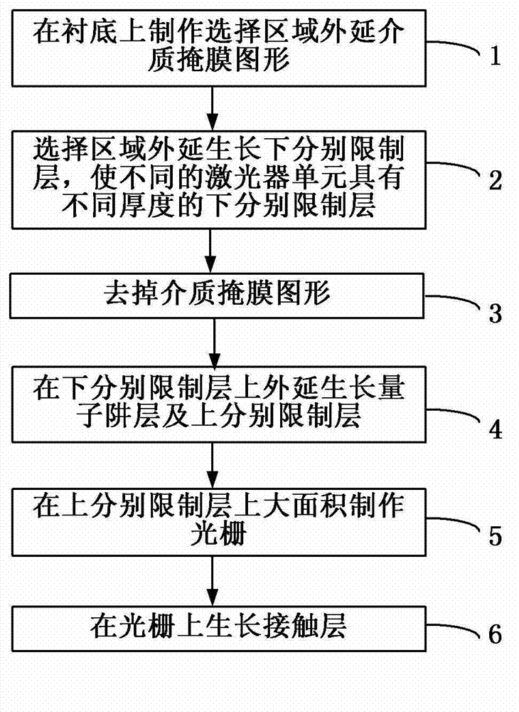
[0038] see again figure 2 , Figure 4 , Figure 5 and Image 6 As shown, the present invention also provides a method (second embodiment) for making a distributed feedback laser array using the selective area epitaxy technique, comprising the following steps:
[0039] Step 1: making a selective area epitaxial dielectric mask pattern 4 on the substrate 1 ( Figure 5 ) or 5( Image 6 ). The substrate 1 is a GaAs substrate, an InP substrate, a GaN substrate, a SiC substrate, a Si substrate, or other III-V, II-VI group material substrates. The period of the dielectric mask pair in mask pattern 4 or 5 and the period of the array unit ( Figure 4 ) are the same, both are S. mask pattern 4 ( Figure 5 ) The distance between the mask pairs remains unchanged, and the mask width gradually increases, that is, the mask M 1 , M 2 , M 3 to M N The width satisfies W 1 2 3 N . mask pattern 5( Image 6 ) in which the mask width remains constant and the mask pair spacing gradual...
PUM
 Abstract
Description
Claims
Application Information


