
A device and method for detecting abnormal welding of electrostatic discharge protection chips

A technology for electrostatic discharge protection and chip welding, which is applied to measuring devices, measuring electricity, measuring electrical variables, etc., which can solve the problems of difficult front and back marks of ESD protection chips, abnormal signals on LCD panels, and poor product assembly, saving manpower. Material cost, reduce the loss of defective rate, high accuracy

Active Publication Date: 2014-10-22
TCL CHINA STAR OPTOELECTRONICS TECH CO LTD
View PDF7 Cites 0 Cited by
  • Summary
  • Abstract
  • Description
  • Claims
  • Application Information

AI Technical Summary

Problems solved by technology

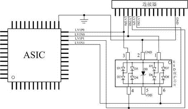
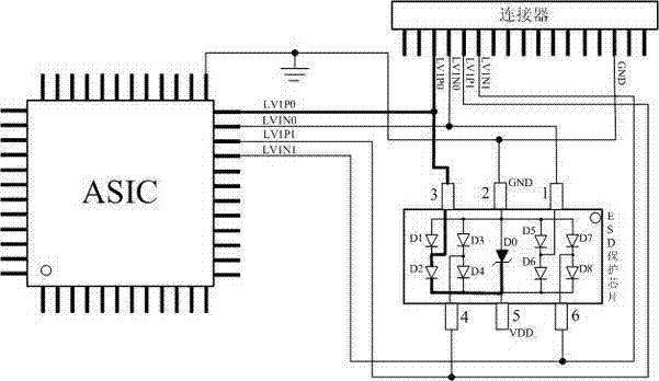
[0010] Still take the transmission of the LV1P0 signal from the connecting pin to the ASIC as an example. When the ESD protection chip is soldered and flipped on the PCB, its signal transmission route is shown in the black thick line in the figure, and the normal LVDS signal is input from the LV1P0 pin of the connector. At this time, the transmitted signal flows into the ground wire after passing through the diode D1. At this time, the voltage distortion at the pin LV1P0 in the ASIC is equal to the U of the conduction voltage drop of the diode D1. D+ , resulting in an abnormal signal output to the LCD panel, resulting in an abnormal display screen
[0011] Since the existing judgment of whether the ESD protection chip is abnormally welded can only be realized by human eyes, but the positive and negative marks of the ESD protection chip are difficult to distinguish, so it is difficult to distinguish abnormal products (products with abnormal welding) from normal products ( Soldering correct product) separated, which will lead to poor assembly of the product

Method used


Image

  • A device and method for detecting abnormal welding of electrostatic discharge protection chips
  • A device and method for detecting abnormal welding of electrostatic discharge protection chips
  • A device and method for detecting abnormal welding of electrostatic discharge protection chips

Examples


Embodiment Construction

[0042] Preferred embodiments of the present invention will be described below with reference to the accompanying drawings.

[0043] Such as Figure 5 As shown, it is a structural schematic diagram of an embodiment of the device for detecting abnormal bonding of ESD protection chips according to the present invention. From Figure 5 It can be seen from the figure that the device for detecting abnormal welding of electrostatic discharge protection chips includes:

[0044] The connector is used for plug-in connection with the signal input connector of the ASIC in the TFT-LCD;

[0045] The detection circuit is arranged on the connector, and is used for detecting whether the ESD protection chip is correctly welded on the ASIC, and prompting when the ESD protection chip is abnormally welded.

[0046] Wherein, a ground connection terminal (GND) and at least one LVDS connection terminal are provided inside the connector, and one end of the ground connection terminal is used to conn...


PUM


Abstract

Disclosed in an embodiment of the present invention is a device for detecting the welding abnormality of an electronic static discharge protection chip, the device comprising: a connector in a plug-in type connection with another connector at the signal input end of an application specific integrated circuit (ASIC) chip in a liquid crystal display; and a detection circuit disposed on the connector to detect whether the electronic static discharge protection chip is properly welded on the ASIC chip, and to give a prompt when the electronic static discharge protection chip is welded abnormally. Correspondingly, also disclosed in the embodiment of the present invention is a method for detecting the welding abnormality of an electronic static discharge protection chip. The embodiment of the present invention can quickly detect with high accuracy whether an electronic static discharge protection chip is welded abnormally, thus saving manpower and material resources and reducing losses caused by the defective product rate during finished product assembly.

Description

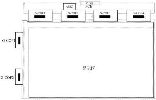
technical field [0001] The invention relates to thin film transistor liquid crystal display technology (Thin Film Transistor Liquid Crystal Display, TFT-LCD), in particular to a device and method for detecting abnormal welding of electrostatic discharge protection chips applied in TFT-LCD. Background technique [0002] TFT-LCD has become a very important display platform in modern information technology and video products. Such as figure 1 As shown, a typical TFT-LCD architecture is shown. The main driving principle of TFT-LCD is: the main board of the control system connects the R / G / B (red / green / blue) compressed signal, control signal and power to the connection on the printed circuit board (PCB) board through the wire. Connector (connector), so that the LCD panel (display area) can obtain the required power and signal. [0003] The signal transmitted to the PCB board through the connector is mainly in the Low Voltage Differential Signaling (LVDS) format, in which every ...

Claims


Application Information

Patent Timeline
Patent Type & Authority Patents(China)
IPC IPC(8): G01R31/02
CPCG01R31/02G02F1/133G01R31/71
Inventor 邓明锋蔡荣茂文松贤庄益壮
Owner TCL CHINA STAR OPTOELECTRONICS TECH CO LTD
Learn More