

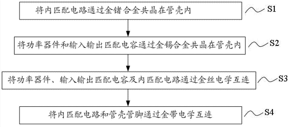
Packaging method of high frequency internal matching power device
A technology of power devices and packaging methods, which is applied in the manufacture of semiconductor devices, electric solid devices, semiconductor/solid devices, etc., and can solve the problem of high Q value of the input matching circuit of internal matching devices, reducing the input VSWR of internal matching devices, and internal matching Problems such as the influence of device output power, to achieve the effect of improving input standing wave ratio, flexible adjustability, and improving input and output impedance
- Summary
- Abstract
- Description
- Claims
- Application Information
AI Technical Summary
Problems solved by technology
Method used
Image

Examples
Embodiment 1
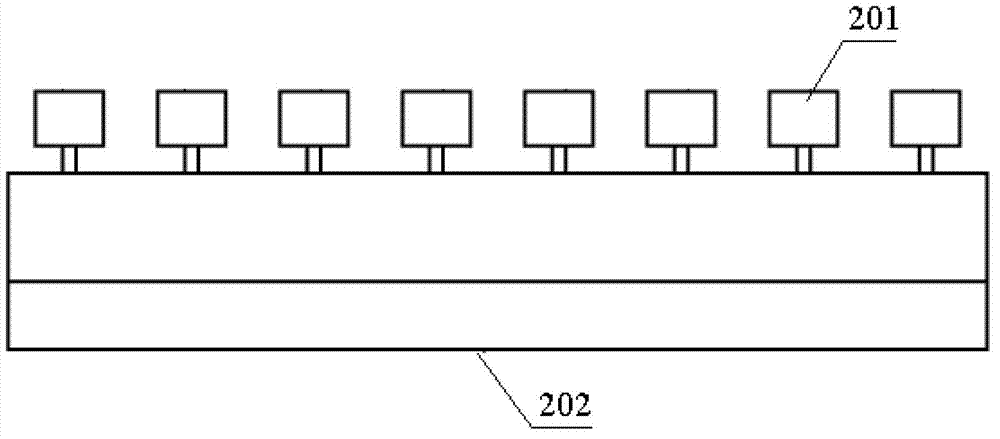
[0048] Such as figure 2 As shown, the upper and lower electrodes are input electrodes 201 and output electrodes 202 respectively, which are respectively used to connect the input and output internal matching circuits for constituting the internal matching circuit. The backside has an electroplated backgold for soldering power devices to the case with AuSn solder. The power device is an AlGaN / GaN HEMTs microwave power device based on a SiC substrate with a total gate width of 6 mm.
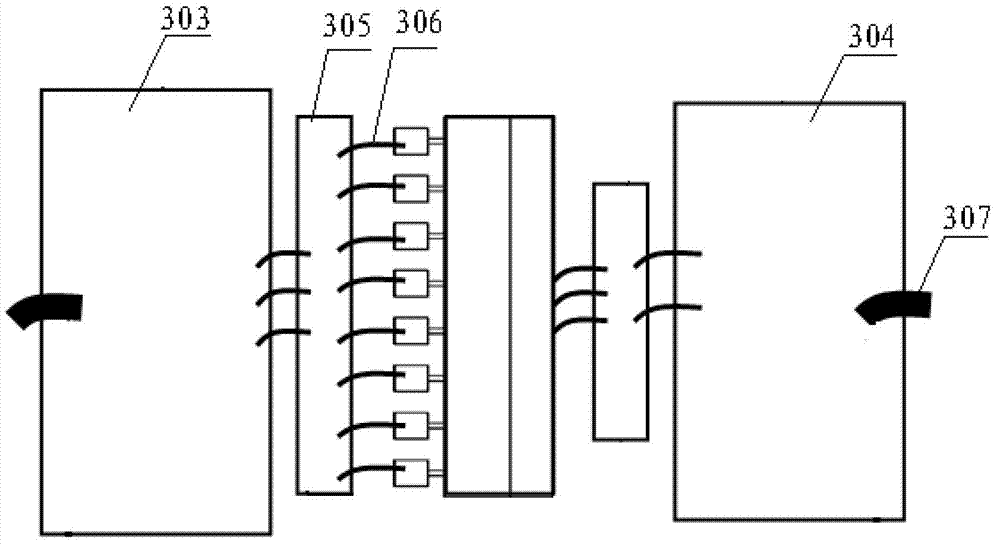
[0049] Such as image 3 As shown, the traditional single-stage LCL internal matching circuit is composed of an input internal matching ceramic circuit 303 and an output internal matching ceramic circuit 304. The input matching of this device adopts a single-stage single-stage circuit consisting of an input matching ceramic capacitor 305 and a gold wire 306 connected in parallel to ground. The LCL network increases the input impedance of the power device, and then the 6mm high-frequency power dev...
Embodiment 2
[0056] The only difference between this embodiment and Embodiment 1 is that the input and output matching capacitors are composed of two input matching chip capacitors and one output matching chip capacitor. Other places are completely consistent with Embodiment 1.
PUM
 Abstract
Description
Claims
Application Information