Compound soft die for wafer-grade nano imprinting of uneven substrate and manufacturing method

A substrate wafer, nano-imprinting technology, applied in the process of producing decorative surface effects, manufacturing microstructure devices, photoplate process of patterned surface, etc. Wafer-level nanoimprint process requirements and other issues to achieve good large-area conformal contact, high resistance to deformation, and ensure consistency

Active Publication Date: 2013-01-02
QINGDAO TECHNOLOGICAL UNIVERSITY
View PDF5 Cites 29 Cited by
  • Summary
  • Abstract
  • Description
  • Claims
  • Application Information

AI Technical Summary

Problems solved by technology

[0003] The purpose of the present invention is to provide a composite soft mold and manufacturing method for non-flat substrate wafer-level nano-imprinting, which solves the problem that existing molds are difficult

Method used


Image

  • Compound soft die for wafer-grade nano imprinting of uneven substrate and manufacturing method
  • Compound soft die for wafer-grade nano imprinting of uneven substrate and manufacturing method
  • Compound soft die for wafer-grade nano imprinting of uneven substrate and manufacturing method

Examples


Embodiment Construction

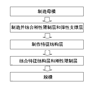
[0038] The present invention will be further described below in conjunction with the accompanying drawings and embodiments.

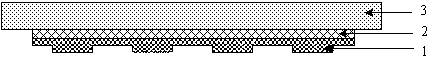
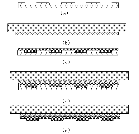
[0039] figure 1 Among them, the composite soft mold for non-flat substrate wafer-level nanoimprinting in this embodiment includes: a characteristic structure layer 1, a rigid confinement layer 2, and an elastic support layer 3; wherein, the characteristic structure layer 1 has a low surface energy, The characteristics of high elastic modulus, high hardness and transparency; the rigid limiting layer 2 has the characteristics of transparency and high elastic modulus; the elastic support layer 3 has the characteristics of transparency and high elasticity. The characteristic structure layer 1 includes the micro-nano pattern structure to be replicated; the rigid confinement layer 2 is located on the characteristic structure layer 1, limiting the lateral deformation and longitudinal deformation of the characteristic structure layer 1; the elastic support laye...


PUM

PropertyMeasurementUnit
Thicknessaaaaaaaaaa
Thicknessaaaaaaaaaa
Thicknessaaaaaaaaaa

Abstract

The invention discloses a compound soft die for wafer-grade nano imprinting of an uneven substrate and a manufacturing method. The compound soft die comprises a characteristic structure layer, a rigid limiting layer and an elastic supporting layer, wherein the characteristic structure layer comprises a micro-nano image structure needing to be copied and is made of a transparent fluorine polymer based material; the rigid limiting layer is located on the characteristic structure layer to limit transverse deformation and vertical deformation of the characteristic structure layer; and the elastic supporting layer is located on the rigid limiting layer. The manufacturing method of the compound soft die comprises the following steps of: (1) manufacturing a female die; (2) manufacturing the rigid limiting layer and the elastic supporting layer, and combining the rigid limiting layer with the elastic supporting layer; (3) manufacturing the characteristic structure layer; (4) combining the characteristic structure layer with the rigid limiting layer; and (5) de-molding. The compound soft die disclosed by the invention has the obvious advantages of high precision, large area, commonly-formed contact capability with the uneven substrate, easiness for de-molding and long service life; and the compound soft die is particularly suitable for a wafer-grade nano imprinting technology of the uneven substrate with a large size and a high resolution.

Description

technical field [0001] The invention relates to a nanoimprint soft mold structure and a manufacturing method thereof, in particular to a composite soft mold structure and a manufacturing method for a large-size non-flat substrate wafer-level nanoimprint process, and belongs to the field of micro-nano manufacturing technology . Background technique [0002] Nanoimprint Lithography (NIL) is a new method of micro-nano patterning. It is a technology that uses a mold to realize its patterning through the force deformation of the resist. Compared with other micro-nano manufacturing methods, NIL has the characteristics of high resolution, ultra-low cost (the international authoritative organization evaluates that NIL at the same production level is at least an order of magnitude lower than traditional optical projection lithography) and high productivity, especially in large-area micro-nano It has outstanding advantages in the manufacture of nanostructures and complex three-dimens...

Claims


Application Information

Patent Timeline
IPC IPC(8): G03F7/00B81C1/00
Inventor 兰红波
Owner QINGDAO TECHNOLOGICAL UNIVERSITY
Why Eureka
Try Eureka