Surface-conduction electron emission source based on graphene

A technology for conducting electrons and secondary electron emission, applied in circuits, electrical components, parts of discharge tubes/lamps, etc., can solve the problems of increasing the complexity of driving circuits, low electron emission efficiency, low emission efficiency, etc. The effect of improved emission efficiency, low cost and simple process

Inactive Publication Date: 2013-01-02
FUZHOU UNIV
View PDF3 Cites 14 Cited by
  • Summary
  • Abstract
  • Description
  • Claims
  • Application Information

AI Technical Summary

Problems solved by technology

[0006] (2) Low electron emission efficiency: Since the electron emission gap is only a few nanometers wide, many electrons are collected by the grid before being extracted by the anode electric field, which leads to low emission efficiency
However, if the gap is increased, a higher voltage is required to emit electrons, which will increase the complexity of the driving circuit

Method used


Image

  • Surface-conduction electron emission source based on graphene
  • Surface-conduction electron emission source based on graphene
  • Surface-conduction electron emission source based on graphene

Examples


no. 1 example

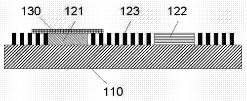
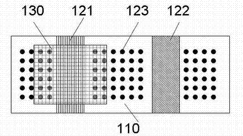
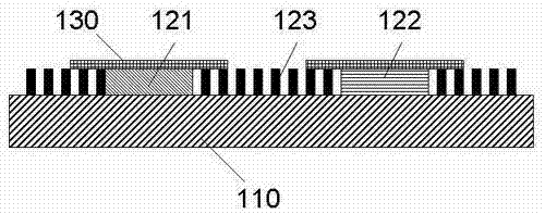
[0032] Step 1, refer to Figure 8 , forming electrodes 121 and 122 on the surface of the substrate 110, the first embodiment of the present invention preferably adopts photosensitive silver paste electrodes, and the specific process includes:

[0033] (a) Spin coating of photosensitive silver paste. The photosensitive silver was transferred to the surface of the substrate 110 by using a spin-coating process, and kept at 110° C. for 20 minutes. The used substrate can be selected from glass, quartz, pottery, and high-temperature-resistant materials with an insulating layer on the surface.

[0034] (b) Exposure. The pre-dried photosensitive silver paste film layer is naturally cooled to room temperature before exposure, and the mask plate of the cathode pattern is covered on the photosensitive silver paste film layer. The photosensitizer of the photosensitive silver paste is negative, so the pattern subjected to ultraviolet light is exposed Light curing, graphics that are not ...


PUM


Abstract

The invention relates to the technical field of surface-conduction electron emission panel display, in particular to a surface-conduction electron emission source based on graphene. The surface-conduction electron emission source comprises a substrate and two electrodes arranged on the surface of the substrate in parallel, nanometer material layers are arranged in a gap between the two electrodes and outer sides of the two electrodes, a graphene film element is respectively arranged on upper portions of the two electrodes or is arranged on the upper portion of one of the electrodes, and one or two sides of each graphene film element extends outwards. The surface-conduction electron emission source has the advantages that a surface-conduction field emission structure, high electron emission performance of the graphene and secondary electron emission performance of a nanometer material array are effectively combined, the graphene in the surface-conduction electron emission source is used as an electron emission source, and the nanometer material array not only is used as a surface electron conductive layer, but also is used as a support for the graphene; and the surface-conduction electron emission source is low in working voltage, high in electron emission efficiency, stable and reliable in emission and simple in manufacturing process.

Description

technical field [0001] The invention relates to the technical field of surface conduction electron emission flat panel display, in particular to a graphene-based surface conduction electron emission source. Background technique [0002] Surface-conduction Electron-emitter Display (SED) is a planar field emission cathode structure. As a display with superior performance, its manufacturing process does not require high-cost and high-precision semiconductor technology. It is produced under ordinary conditions; and the surface conduction emitter it has is a planar field emission structure, and the emission performance is much more stable. The history of the surface conduction electron emission phenomenon can be traced back to the early 1960s, when it was discovered by former Soviet scholars, and it was generally classified as thin film field emission. The key part of SED is the manufacture of the lower substrate, that is, the surface conduction field emission cathode, which is ...

Claims


Application Information

Patent Timeline
Patent Type & Authority Applications(China)
IPC IPC(8): H01J1/304
Inventor 李福山郭太良吴朝兴张永志寇丽杰张蓓蓓
Owner FUZHOU UNIV
Why Eureka
Try Eureka