MOSFET (metal oxide semiconductor field effect transistor) and manufacturing method thereof

A manufacturing method, semiconductor technology, applied in the direction of semiconductor/solid-state device manufacturing, semiconductor devices, electrical components, etc.

Active Publication Date: 2015-02-11
INST OF MICROELECTRONICS CHINESE ACAD OF SCI
View PDF5 Cites 0 Cited by
  • Summary
  • Abstract
  • Description
  • Claims
  • Application Information

AI Technical Summary

Problems solved by technology

[0004] However, the above-mentioned SOI MOSFET with a back gate must be grounded or biased at a predetermined potential during operation, thus requiring additional chip area for providing an electrical contact to the back gate, for example for forming additional channels and wiring

Method used


Image

  • MOSFET (metal oxide semiconductor field effect transistor) and manufacturing method thereof
  • MOSFET (metal oxide semiconductor field effect transistor) and manufacturing method thereof
  • MOSFET (metal oxide semiconductor field effect transistor) and manufacturing method thereof

Examples


Embodiment Construction

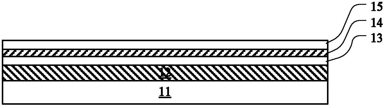
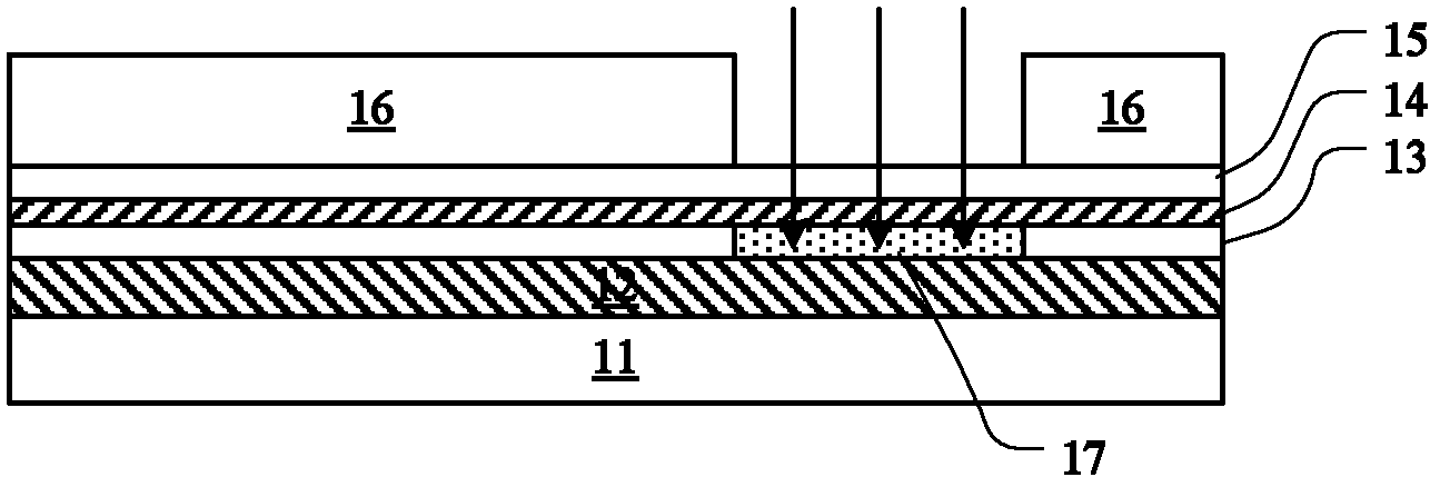
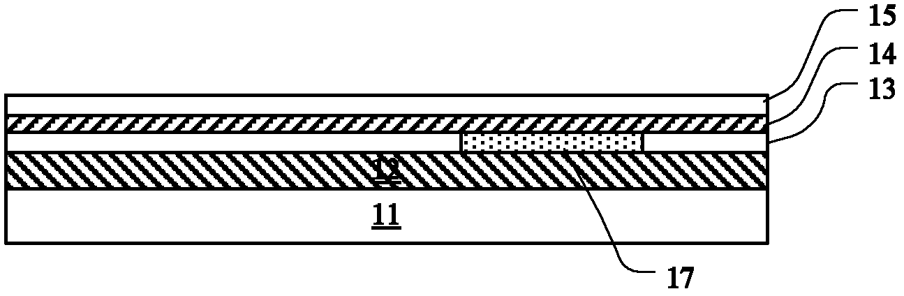
[0015] Hereinafter, the present invention will be described in more detail with reference to the accompanying drawings. In the various figures, identical elements are indicated with similar reference numerals. For the sake of clarity, various parts in the drawings have not been drawn to scale.

[0016] In the following, many specific details of the present invention are described, such as device structures, materials, dimensions, processing techniques and techniques, for a clearer understanding of the present invention. However, the invention may be practiced without these specific details, as will be understood by those skilled in the art. Unless otherwise specified below, various parts in the semiconductor device may be composed of materials known to those skilled in the art.

[0017] In this application, the term "semiconductor structure" refers to the general designation of the entire semiconductor structure formed in various steps of manufacturing a semiconductor device...


PUM


Abstract

Provided are a MOSFET and a manufacturing method therefor. The MOSFET comprises: a semiconductor substrate, a first buried insulating layer on the semiconductor substrate, a backgate formed within a first semiconductor layer on the first buried insulating layer, a second buried insulating layer on the first semiconductor layer, source / drain regions formed within a second semiconductor layer on the second buried insulating layer, a gate on the second semiconductor layer, and an electrical connection of the source / drain regions, the gate, and the backgate. The backgate is only arranged below one in the source / drain regions and below a channel region, and not below the other in the source / drain regions. The electrical connection comprises a public conductive channel of the backgate and of the one in the source / drain regions. The MOSFET uses asymmetric backgate to improve the suppression of a short-channel effect, and uses the public conductive channel to reduce chip footprint.

Description

technical field [0001] The present invention relates to a MOSFET and a manufacturing method thereof, more particularly, to a MOSFET with a back gate and a manufacturing method thereof. Background technique [0002] An important development direction of integrated circuit technology is to scale down the size of metal-oxide-semiconductor field-effect transistors (MOSFETs) to improve integration and reduce manufacturing costs. However, it is well known that short-channel effects occur as the size of MOSFETs decreases. As the size of the MOSFET is scaled down, the effective length of the gate is reduced, so that the proportion of depletion layer charge that is actually controlled by the gate voltage is reduced, so that the threshold voltage decreases as the channel length decreases. [0003] Yan et al. proposed in "Scaling the Si MOSFET: From bulk to SOI to bulk" (IEEE Trans. Elect. Dev., Vol. 39, p. 1704, July 1992), in SOI MOSFET, by A ground plane (that is, a grounded back ...

Claims


Application Information

Patent Timeline
Patent Type & Authority Patents(China)
IPC IPC(8): H01L21/336H01L21/28H01L29/78H01L29/06H01L29/423
CPCH01L29/78603H01L29/78648H01L29/66772H01L21/76264
Inventor 朱慧珑梁擎擎尹海洲骆志炯
Owner INST OF MICROELECTRONICS CHINESE ACAD OF SCI
Why Eureka
Try Eureka