Manufacture method of array type high-voltage LED device

A technology of LED device and manufacturing method, applied in the semiconductor field

Inactive Publication Date: 2013-01-09
INST OF SEMICONDUCTORS - CHINESE ACAD OF SCI
View PDF5 Cites 30 Cited by
  • Summary
  • Abstract
  • Description
  • Claims
  • Application Information

AI Technical Summary

Problems solved by technology

The current DC LED products have some disadvantages in the application, such as needing to be used together with transformers and other original components, and the lifespan is only about 20,000 hours, while the lifespan of the actual LED chip is as long as 50,000-100,000 hours

Method used


Image

  • Manufacture method of array type high-voltage LED device
  • Manufacture method of array type high-voltage LED device
  • Manufacture method of array type high-voltage LED device

Examples


Embodiment

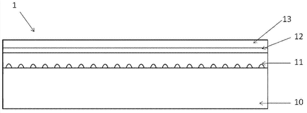
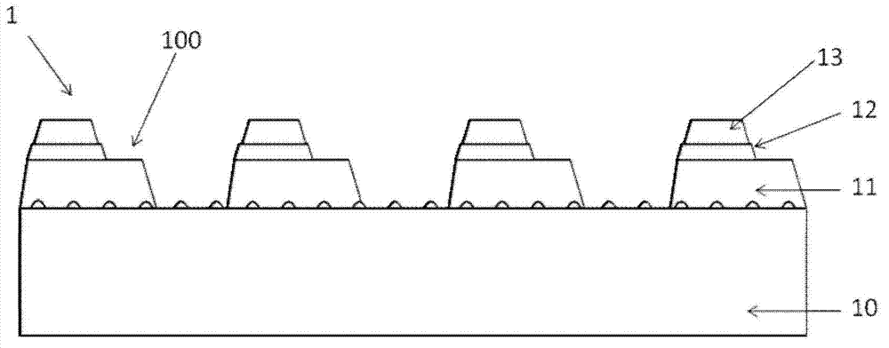
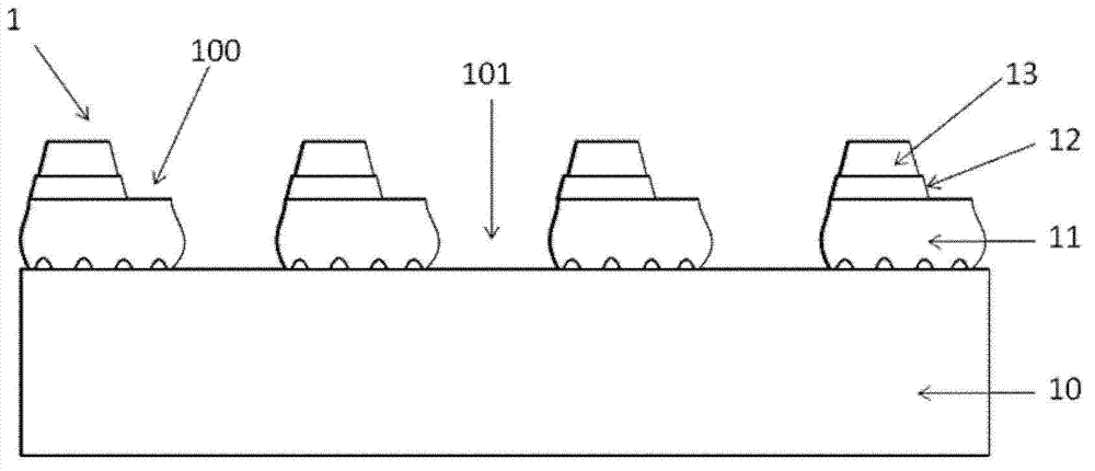
[0035] see Figure 1 to Figure 6 As shown, the present invention provides a method for manufacturing a high-efficiency array type high-voltage LED device comprising:

[0036] Step 1: Take an epitaxial structure 1, the epitaxial structure 1 includes a substrate 10, an N-type gallium nitride layer 11, an active layer 12 and a P-type gallium nitride layer 13;

[0037] Step 2: use photolithography to make a mask, and ICP etch the epitaxial structure to the N-type GaN layer 11 with an etching depth of 1.5 μm to form N-type steps;

[0038] Step 3: Grow SiO with a thickness of 2um by PECVD 2 , using a photolithography method to make a mask, etching silicon dioxide, and using an ICP deep etching method to etch part of the epitaxial region to the substrate 10 to form an isolation deep groove;

[0039] Step 4: heating the sulfur-phosphoric acid mixed solution to 250° C., and subjecting the epitaxial material to high-temperature sulfuric-phosphoric acid etching for 5 minutes;

[0040]...


PUM

PropertyMeasurementUnit
thicknessaaaaaaaaaa
thicknessaaaaaaaaaa
thicknessaaaaaaaaaa

Abstract

The invention discloses a manufacture method of an array type high-voltage LED device, which comprises the steps of: manufacturing a mask on a P type gallium nitride layer with an epitaxial structure, selectively etching the epitaxial structure to form an N type step structure; manufacturing a mask on the surface of an N type gallium nitride layer with an epitaxial structure, forming isolated deep trench; carrying out high-temperature sulfur phosphoric acid corrosion; depositing an insulation dielectric layer on the surface of the etched epitaxial structure; corroding the insulation dielectric layer outside the side wall of the deep trench; manufacturing a transparent conductive layer between adjacent N type step structures; partially corroding the transparent conductive layer on the surface of the P type gallium nitride layer on the N type step structure on the outermost side; and manufacturing a P metal electrode and an N metal electrode on the transparent conductive layer. According to the invention, electrode light absorption can be reduced, the light outlet area on the epitaxial side surface and the bottom of the chip is increased, the manufacture method is mutually matched with a post process, and thus the light emitting efficiency of a high-voltage LED chip can be increased.

Description

technical field [0001] The invention belongs to the technical field of semiconductors, in particular to a method for manufacturing an array type high-voltage LED device with high light efficiency. Background technique [0002] Due to the advent of the oil energy crisis, more and more attention has been paid to the development of more efficient and power-saving electronic and lighting equipment. Under this trend, it has the advantages of power saving, environmental protection (mercury-free), no pollution, long life, high brightness, and responsiveness. Light-Emitting Diode (LED) components, which have the advantages of high speed, small size, and high luminous efficiency, have gradually emerged in the lighting industry, and their application range is widespread in daily life, such as indicator lights on instrument panels. [0003] HV LED is to separate a certain number of microcrystalline grains on the original DC LED chip, and then interconnect the microcrystalline grains th...

Claims


Application Information

Patent Timeline
Patent Type & Authority Applications(China)
IPC IPC(8): H01L27/15
Inventor 詹腾张杨李璟刘志强伊晓燕王国宏
Owner INST OF SEMICONDUCTORS - CHINESE ACAD OF SCI
Why Eureka
Try Eureka