Film ablation sensor and manufacturing method thereof

A sensor and film technology, applied in the direction of material resistance, can solve the problems of complex production process of ablation sensors and low sensor reliability, and achieve the effects of improving consistency, improving processing efficiency and reducing manufacturing costs.

Active Publication Date: 2014-08-20
48TH RES INST OF CHINA ELECTRONICS TECH GROUP CORP
View PDF8 Cites 0 Cited by
  • Summary
  • Abstract
  • Description
  • Claims
  • Application Information

AI Technical Summary

Problems solved by technology

[0008] The purpose of the present invention is to provide a thin-film ablation sensor and its preparation method for the defects of complex production process and low reliability level of the ablation sensor in the prior art. The production process of the sensor is simple and mature, and it has good anti-environmental interference Capability and Reliability Levels

Method used


Image

  • Film ablation sensor and manufacturing method thereof
  • Film ablation sensor and manufacturing method thereof
  • Film ablation sensor and manufacturing method thereof

Examples


Embodiment 1

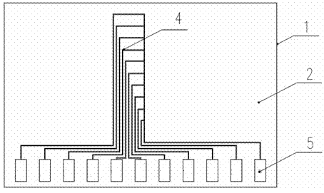
[0035] see Figure 1 to Figure 5 , the thin film ablation sensor 1 includes a substrate 2, a transition layer 3 disposed on the substrate 2, an ablation resistor 4 disposed on the transition layer 3; a protective film 6 is provided on the ablation resistor 4; The corrosion resistance 4 is a resistance sequence composed of more than two resistances; the resistance includes a lead wire welding panel 5; the lead welding panel 5 is connected to the adapter plate 13 through a lead 10; the base 2 is provided with a height Adjustment hole 9;

[0036] Wherein, the material of the base 2 is Al 2 o 3 , with a diameter of 50 mm to 150 mm and a thickness of 0.5 mm to 1 mm; the material of the transition layer 3 is Ta 2 o 5 , with a thickness of 0.05 μm to 0.1 μm; the material of the ablation resistor 4 is Au, and its thickness is 0.2 μm to 0.5 μm; the material of the protective film 6 is SiO 2 , the thickness is 0.1μm~0.2μm. The height adjustment hole 9 is a through hole of 1.6mm×10...

Embodiment 2

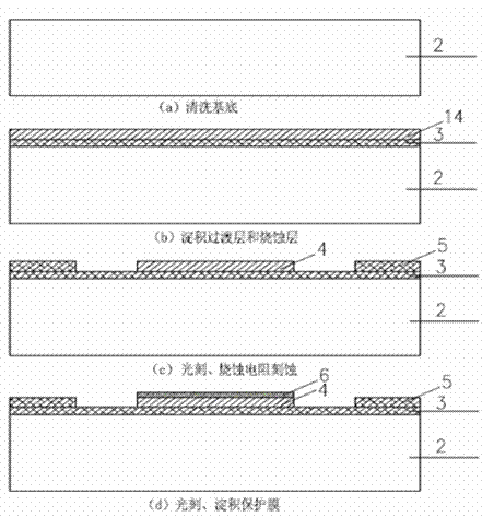
[0038] (1) For Al with a diameter of 50mm~150mm and a thickness of 0.5mm~1mm 2 o 3 The substrate 2 is cleaned to remove oil and impurities on the polished surface of the substrate;

[0039](2) Deposit Ta with a thickness of 0.05 μm to 0.1 μm by ion beam sputtering 2 o 5 The transition film 3 is used to enhance the bonding force between the Au thin film layer and the base layer 2;

[0040] (3) Ion beam sputtering deposits an Au thin film layer with a thickness of 0.2 μm to 0.5 μm, which is the ablation material layer 14 ;

[0041] (4) Make and ablate the photoresist mask layer in the shape of a resistor on the Au film by photolithography, and use iodine and potassium iodide etching solution to etch the Au film to remove the unnecessary Au film area to form an Au film ablation Resistor 4 and lead welding area 5;

[0042] (5) Make a photoresist mask layer by photolithography process to protect the lead welding area;

[0043] (6) Ion beam sputtering deposits SiO with a thick...


PUM

PropertyMeasurementUnit
diameteraaaaaaaaaa
thicknessaaaaaaaaaa
thicknessaaaaaaaaaa

Abstract

The invention discloses a thin-film ablation sensor and a preparation method thereof. The thin-film ablation sensor comprises a substrate, a transition layer arranged on the substrate, and an ablation resistor arranged on the transition layer; the ablation resistor includes wire welding The panel area; the lead wire welding panel area is connected to the adapter plate through the lead wire; the ablation resistor is provided with a protective film; the base is provided with a height adjustment hole. The invention adopts micro-machining technology to prepare the film ablation sensor. The thin film ablation sensor according to the invention has a simple manufacturing process and can meet different measurement accuracy requirements.

Description

technical field [0001] The invention belongs to the technical field of ablation sensors, and in particular relates to a thin-film ablation sensor based on micromachining technology and a preparation method thereof. More specifically, the present invention relates to a thin-film ablation sensor and a preparation method thereof. The measurement of the ablation rate of the heat insulating layer is realized through the thin-film resistance. The manufacturing process of the thin-film ablation sensor is simple and has high measurement accuracy. Background technique [0002] The heat insulation layer is mainly used in the thermal protection of solid rocket motors, re-entry vehicles and other spacecraft. The performance of the heat insulation layer directly affects the reliability of the engine, and even affects the success or failure of the rocket launch. [0003] The working environment of the heat insulation layer is very harsh. It has to withstand the ablation of high temperatur...

Claims


Application Information

Patent Timeline
Patent Type & Authority Patents(China)
IPC IPC(8): G01N27/04
Inventor 景涛谢贵久颜志红张建国
Owner 48TH RES INST OF CHINA ELECTRONICS TECH GROUP CORP
Why Eureka
Try Eureka