Mixed-structure field effect transistor and manufacturing method thereof

A technology of field-effect transistors and hybrid structures, which is applied in the manufacture of semiconductor/solid-state devices, semiconductor devices, electrical components, etc., can solve the problems of large channel resistance of SiC MOSFET, and achieve the effect of solving the effect of large inversion channel resistance

Active Publication Date: 2015-04-22
SUN YAT SEN UNIV
View PDF6 Cites 0 Cited by
  • Summary
  • Abstract
  • Description
  • Claims
  • Application Information

AI Technical Summary

Problems solved by technology

[0008] The purpose of the present invention is to solve the problem of GaN HFET normally-off device and vertical device preparation, and at the same time solve the problem of SiC MOSFET channel resistance

Method used


Image

  • Mixed-structure field effect transistor and manufacturing method thereof
  • Mixed-structure field effect transistor and manufacturing method thereof
  • Mixed-structure field effect transistor and manufacturing method thereof

Examples


Embodiment 1

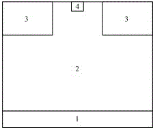
[0052] figure 1 It is a structural schematic diagram of Embodiment 1 of the present invention, Figure 2 to Figure 8 It is the process schematic diagram of embodiment 1.

[0053] Such as figure 2 First, grow the SiC epitaxial layer 2 on the SiC substrate 1. The SiC epitaxial layer 2 may include a buffer layer with a higher doping concentration. The doping concentration and thickness of the SiC epitaxial layer 2 are set according to the withstand voltage requirements. The selection of SiC substrate 1 can be of the same conductivity type as SiC epitaxial layer 2. At this time, the invention is a unipolar device, similar to a power MOSFET; it can also be of a different conductivity type from SiC epitaxial layer 2. At this time , the invention is a bipolar device, similar to an IGBT.

[0054] then follow image 3 , the first region 3 and the second region 4 are formed on the SiC epitaxial layer 2 by ion implantation. The first region 3 is located on both sides of the SiC epi...

Embodiment 2

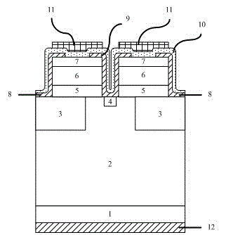
[0061] image 3 It is a structural schematic diagram of Embodiment 2 of the present invention, Figures 10 to 16 It is the process schematic diagram of embodiment 2.

[0062] Such as Figure 10Firstly, a SiC epitaxial layer 2 , a buffer layer 5 , a GaN layer 6 and an AlGaN layer 7 are grown sequentially from bottom to top on a SiC substrate 1 , and then a sacrificial layer 13 is deposited. The choice of the substrate can be of the same conductivity type as the SiC epitaxial layer 2. At this time, the invention is a unipolar device, similar to a power MOSFET; it can also be of a different conductivity type from the SiC epitaxial layer 2. At this time, the invention It is a bipolar device, similar to an IGBT.

[0063] then follow Figure 11 , etch grooves on the buffer layer 5, the GaN layer 6 and the AlGaN layer 7, and then form the first region 3 by ion implantation, wherein the first region 3 is located on both sides of the SiC epitaxial layer 2, and the first region 3 an...

Embodiment 3

[0069] Figure 17 Shown is Embodiment 3 of the present invention, which differs from Embodiment 1 in that the device is a lateral device. The drain 12 is located on the surface of the device, and the contact region 14 between the drain 12 and the SiC epitaxial layer 2 can be of the same conductivity type as the SiC epitaxial layer 2. At this time, the invention is a unipolar device, similar to a power MOSFET; It can be of a different conductivity type from the SiC epitaxial layer 2, at this time, the invention is a bipolar device, similar to an IGBT.


PUM


Abstract

The invention discloses a mixed-structure field effect transistor and a manufacturing method thereof. According to the transistor, a device is controlled to switch on and off by the voltage withstanding of SiC and a heterostructure layer grown epitaxially on a SiC epitaxial layer. According to the mixed-structure field effect transistor, the current collapse effect of the conventional HFET (Heterojunction Field Effect Transistor) is avoided, a device of which the voltage withstanding capacity is better than that of AlGaN / GaN HFET can be manufactured, a threshold voltage is easy to adjust, and a normally off device and a longitudinal device are realized. Simultaneously, compared with a SiC MOS (Metal Oxide Semiconductor) channel, a two-dimensional electron gas channel in the position of the interface of the heterostructure layer has high electronic mobility inside and small channel resistance, so that the advantages of the AlGaN / GaN HFET and the SiC MOSFET (Metal-Oxide -Semiconductor Field Effect Transistor) are combined, and a high-performance power semiconductor switching device is realized.

Description

technical field [0001] The invention relates to the field of semiconductor devices, in particular to a hybrid structure field effect transistor device and a manufacturing method. Background technique [0002] The tradeoff between breakdown voltage, on-resistance and switching speed sets a theoretical limit for power semiconductor devices. As the performance of silicon-based power devices is approaching the theoretical limit, efforts to further improve the performance of power semiconductor devices have shifted to research on new material devices. [0003] The third-generation semiconductors represented by GaN and SiC have become ideal substitutes for the next generation of power switching devices due to their superior properties such as wide bandgap, high breakdown electric field, saturated electron drift velocity, and good thermal conductivity. At present, GaN and SiC devices have different problems, which hinder their commercial development. They are described separately...

Claims


Application Information

Patent Timeline
Patent Type & Authority Patents(China)
IPC IPC(8): H01L29/778H01L29/10H01L29/423H01L21/335
Inventor 刘扬魏进姚尧
Owner SUN YAT SEN UNIV
Why Eureka
Try Eureka