Multi-focus femtosecond laser scribing method applied to separation of light emitting diode (LED) device

A LED device, femtosecond laser technology, applied in laser welding equipment, welding equipment, metal processing equipment, etc., can solve the problems of reduced light transmittance, complicated light-emitting diode preparation process, difficult sapphire substrate, etc.

Inactive Publication Date: 2013-01-23
INST OF SEMICONDUCTORS - CHINESE ACAD OF SCI
View PDF6 Cites 20 Cited by
  • Summary
  • Abstract
  • Description
  • Claims
  • Application Information

AI Technical Summary

Problems solved by technology

However, mechanical thinning and polishing of sapphire will damage the GaN epitaxial layer to a certain extent, thereby reducing the luminous efficiency of light-emitting diodes
At the same time, mechanically thinning and polishing the sapphire substrate will complicate the preparation process of light-emitting diodes, thereby increasing the production cost of the device
Moreover, due to the long nanosecond laser pulse, the high temperature generated by its focus on the sapphire substrate will cause a phase change in the sapphire near the laser scratch, which will reduce the light transmittance near the laser scratch, which also affects the performance of the device. light extraction efficiency
On the other hand, due to cost considerations, the epitaxial wafers of GaN-based light-emitting diodes are undergoing industrial upgrading in the direction of large-scale epitaxy such as 4 inches, 6 inches, and even 8 inches. The huge stress caused by the matching makes it difficult to thin the sapphire substrate to a thickness of about 100 μm

Method used


Image

  • Multi-focus femtosecond laser scribing method applied to separation of light emitting diode (LED) device
  • Multi-focus femtosecond laser scribing method applied to separation of light emitting diode (LED) device
  • Multi-focus femtosecond laser scribing method applied to separation of light emitting diode (LED) device

Examples


Embodiment Construction

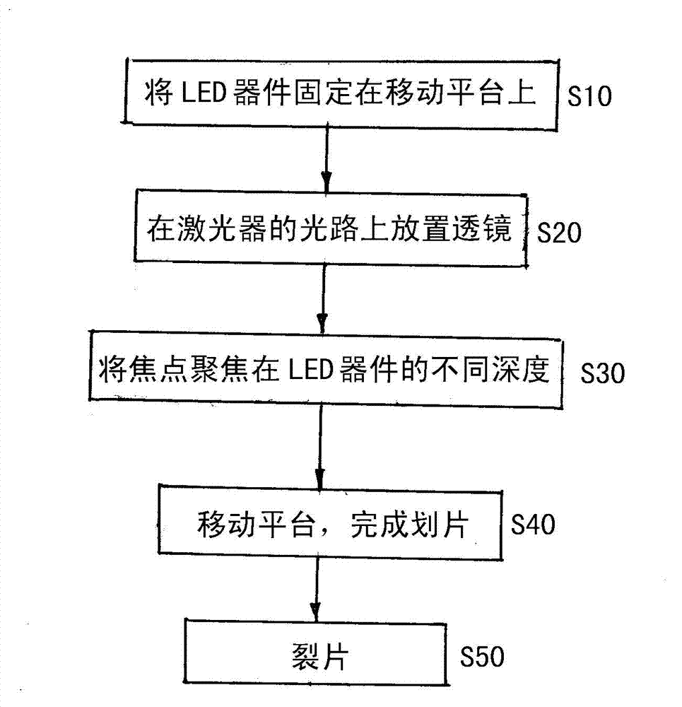
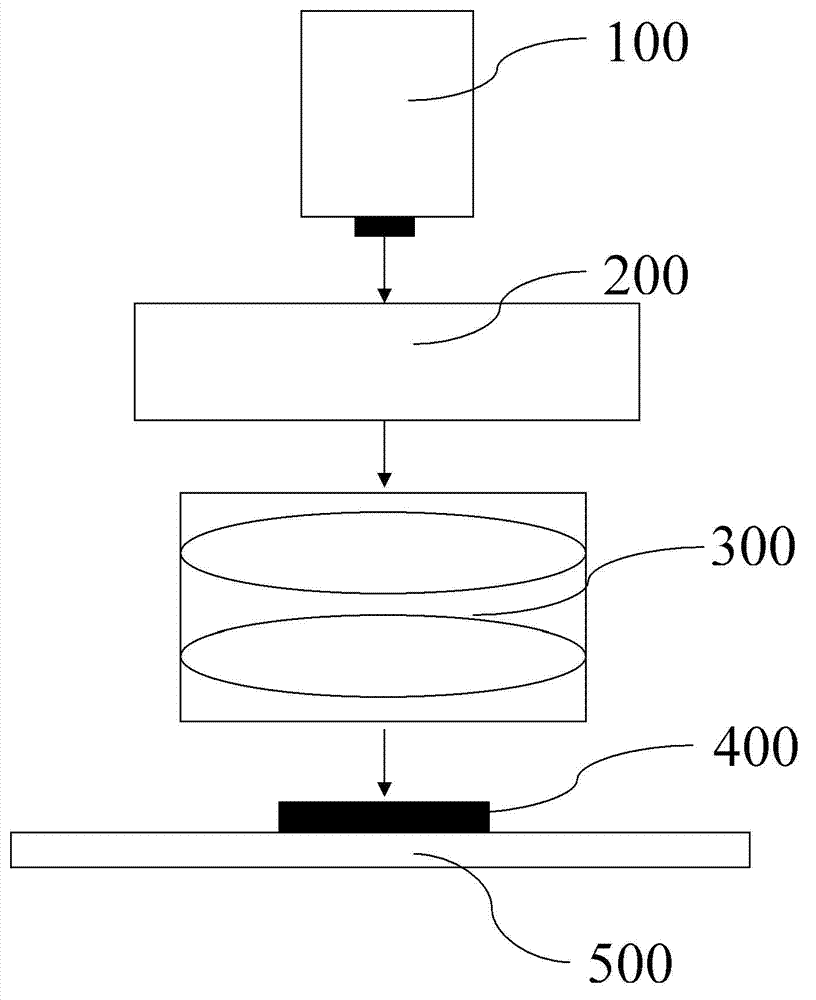
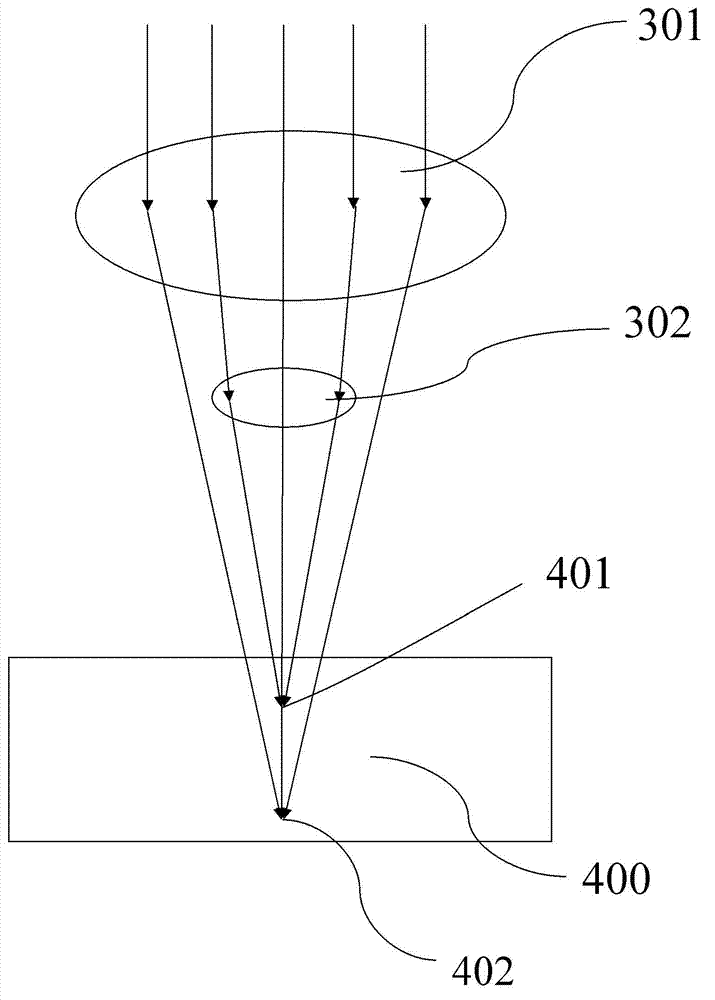
[0019] Please refer to Figure 1 to Figure 3 As shown, the present invention provides a multi-focus femtosecond laser scribing method applied to the separation of LED devices, including:

[0020] Step S10: Fix the prepared LED device 400 on the horizontal moving platform 500, then adjust the CCD focus of the optical path system, so that the back of the LED device 400 is located at the imaging center of the CCD imaging device 200 (see figure 2 ); adjust the horizontal moving platform 500 to be parallel to the runway of the LED device 400 .

[0021] Step S20: placing a plurality of lenses 300 on the laser optical path of the femtosecond laser 100 to divide the laser light into multiple focal points, the central wavelength range of the laser output by the femtosecond laser 100 is 200nm-1600nm, and the pulse width range is 1fs-1000fs, The repetition frequency is 1MHz-1000MHz, the average power range is 1mw-100W, the number of the lens 300 and the focal point is 1-10 (the number ...


PUM

PropertyMeasurementUnit
wavelengthaaaaaaaaaa
poweraaaaaaaaaa
poweraaaaaaaaaa

Abstract

The invention discloses a multi-focus femtosecond laser scribing method applied to separation of light emitting diode (LED) device. The multi-focus femtosecond laser scribing method comprises the following steps of: fixing a prepared LED device on a horizontal mobile platform and positioning the prepared LED device in an imaging center of charge coupled device (CCD) imaging equipment; 2, placing a plurality of lenses on a laser light path of a femtosecond laser, and dividing laser into a plurality of focuses; 3, focusing the focuses on parts in a substrate of the LED device at different depths; 4, transversely and longitudinally moving the horizontal mobile platform, and performing femtosecond laser scribing; and 5, shredding the LED device to obtain a single LED device. By the multi-focus femtosecond laser scribing method, a sapphire substrate can be cut by different light beams simultaneously, and effects that the substrate is cut at one time, and a plurality of scratches are caused are achieved, so that a relatively thick sapphire substrate is cut in a mode that low damage is caused, and the LED device is separated.

Description

technical field [0001] The invention belongs to the technical field of semiconductors, in particular to the technical field of gallium nitride-based light-emitting diode wafer laser scribing technology. Background technique [0002] Laser scribing technology is widely used in the device separation process of gallium nitride-based light-emitting diode wafers, which is simple, fast and efficient. Now the ordinary nanosecond laser scribing machine can only leave cutting marks with a depth of 20 μm to 50 μm on the sapphire substrate when cutting the sapphire substrate for device separation. In this way, the sapphire substrate with a thickness of about 460 μm needs to be mechanically thinned and polished to a thickness of 70-120 μm before it can be scratched to achieve the purpose of device separation. However, the mechanical thinning and polishing of sapphire will damage the gallium nitride epitaxial layer to a certain extent, thereby reducing the luminous efficiency of the lig...

Claims


Application Information

Patent Timeline
Patent Type & Authority Applications(China)
IPC IPC(8): B23K26/36B23K26/067B23K26/38
Inventor 谢海忠张逸韵杨华李璟伊晓燕王军喜王国宏李晋闽
Owner INST OF SEMICONDUCTORS - CHINESE ACAD OF SCI
Why Eureka
Try Eureka