Metal silicide forming method

A metal silicide, wet etching technology, used in electrical components, semiconductor/solid-state device manufacturing, semiconductor devices, etc., can solve the problem of high device failure rate, reduce the probability of drift, reduce the probability of device failure, The effect of reducing soaking time

Active Publication Date: 2013-02-06
CSMC TECH FAB2 CO LTD
View PDF5 Cites 7 Cited by
  • Summary
  • Abstract
  • Description
  • Claims
  • Application Information

AI Technical Summary

Problems solved by technology

However, after etching with DHF solution, the failure rate of the device is still high

Method used


Image

  • Metal silicide forming method
  • Metal silicide forming method
  • Metal silicide forming method

Examples


Embodiment Construction

[0040] The following will clearly and completely describe the technical solutions in the embodiments of the present invention with reference to the accompanying drawings in the embodiments of the present invention. Obviously, the described embodiments are only some, not all, embodiments of the present invention. Based on the embodiments of the present invention, all other embodiments obtained by persons of ordinary skill in the art without making creative efforts belong to the protection scope of the present invention.

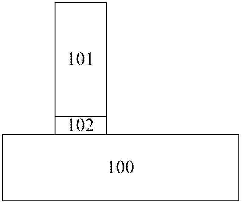
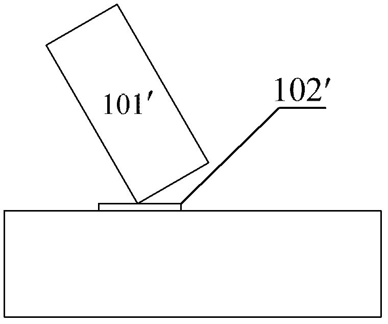
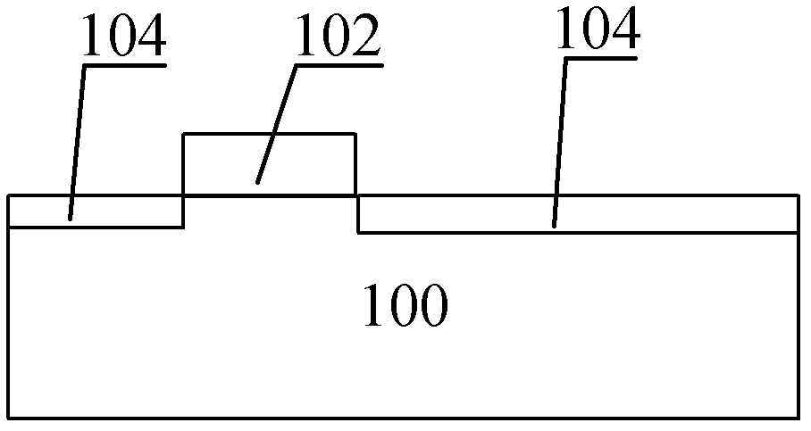
[0041] As mentioned in the background technology section, when the SAB layer is etched with the BOE solution in the traditional process, the BOE solution easily penetrates into the SAB protected by the photoresist through the photoresist, which makes the device prone to short circuit. In the existing technology, DHF solution is used instead of BOE solution. The DHF solution is not easy to penetrate through the photoresist into the SAB protected by the photoresi...


PUM


Abstract

The embodiment of the invention discloses a metal silicide forming method, comprising the following steps: a substrate is provided, and a gate region, a source region and a drain region are formed on the substrate; a metal silicide barrier layer is formed on the substrate; a photoresist layer with a gate region pattern, a source region pattern and a drain region pattern are formed on the metal silicide barrier layer; the photoresist layer with the gate region pattern, the source region pattern and the drain region pattern is used as a mask, the dry method etching process is adopted to etch the metal silicide barrier layer, the metal silicide barrier layer with the preset thickness is reserved, and the preset thickness is formed in the way that the photoresist layer with the gate region pattern, the source region pattern and the drain region pattern is used as the mask, and a primary wet method etching is carried out by adopting the DHF (dilute hydrofluoric acid) solution; the photoresist layer with the gate region pattern, the source region pattern and the drain region pattern is removed; and the metal silicide is formed on the substrate. With the adoption of the metal silicide forming method provided by the invention, the failure rate of a device is reduced.

Description

technical field [0001] The invention relates to the technical field of semiconductor device manufacturing technology, and more specifically, relates to a metal silicide forming method. Background technique [0002] In the manufacturing process of semiconductor devices, the manufacturing process of the device includes steps: (1) formation of gate dielectric layer and gate; (2) LDD (lightly doped drain) lithography and implantation; (3) sidewall formation; (4) ) S / D (source / drain) lithography, implantation; (5) SAB (Salicide Block, metal silicide barrier layer) deposition, lithography, etching; (6) Salicide (silicide) metal process, forming metal contacts . [0003] In the traditional process, BOE solution (a mixed solution of hydrofluoric acid and ammonium fluoride) is often used when etching SAB. The BOE solution easily penetrates into the SAB protected by the photoresist through the photoresist. Corrosion of the protected SAB by the BOE solution will lead to a short circu...

Claims


Application Information

Patent Timeline
Patent Type & Authority Applications(China)
IPC IPC(8): H01L21/28H01L21/336
Inventor 孙晓峰高永亮丁海滨
Owner CSMC TECH FAB2 CO LTD
Why Eureka
Try Eureka