Trenched Schottky-barrier diode and manufacturing method thereof

A Schottky potential and diode technology, which is applied in semiconductor/solid-state device manufacturing, electrical components, circuits, etc., can solve the problems of large reverse leakage, low performance and reliability, poor reverse blocking ability, etc., and achieve low Reverse leakage, reduced requirements for absolute thickness and relative thickness uniformity, effects of high voltage reverse blocking capability

Active Publication Date: 2013-02-06
HANGZHOU LION MICROELECTRONICS CO LTD
View PDF5 Cites 8 Cited by
  • Summary
  • Abstract
  • Description
  • Claims
  • Application Information

AI Technical Summary

Problems solved by technology

[0006] The present invention aims to solve the problems of low performance and reliability, large reverse leakage and poor reverse blocking ability of the trench Schottky barrier diode in the prior art, and provides a low reverse leakage and low voltage reverse resistance Trench Schottky barrier diode with good breaking ability and good reliability

Method used


Image

  • Trenched Schottky-barrier diode and manufacturing method thereof
  • Trenched Schottky-barrier diode and manufacturing method thereof
  • Trenched Schottky-barrier diode and manufacturing method thereof

Examples


Embodiment 1

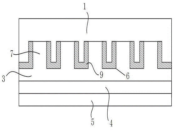
[0046] Such as figure 2 As shown, a trench Schottky barrier diode consists of an anode metal layer 1, a lightly doped epitaxial layer 3 of the first conductivity type, a substrate 4, and a cathode that form an ohmic contact with each other from top to bottom. The metal layer 5 is composed of the substrate 4 and the epitaxial layer 3, both of which are monocrystalline silicon. The upper part of the epitaxial layer 3 is horizontally carved with a number of grooves 6, and the epitaxial layer 3 between adjacent grooves 6 forms a boss 7. The epitaxial layer 3 The impurity doping concentration increases from the top surface to the bottom surface, where the top surface doping concentration is 10 16 cm -3 , the bottom doping concentration is 10 21 cm -3 A Schottky barrier metal layer 2 with a thickness of 10 angstroms is evaporated between the anode metal layer 1 and the epitaxial layer 4, and the Schottky barrier metal layer 2 forms a Schottky barrier contact with the top surfa...

Embodiment 2

[0061] The trench Schottky barrier diode structure of this embodiment is the same as that of Embodiment 1, except that the thickness of the Schottky barrier metal layer 2 in this embodiment is 500 angstroms, and the doping concentration of the top surface of the epitaxial layer 3 is for 10 15 cm -3 , the bottom doping concentration is 10 20 cm -3 , the top surface doping concentration of conductive polysilicon 8 is 10 19 cm -3 , the bottom doping concentration is 10 15 cm -3 .

[0062] The rest of the steps in the method for manufacturing trench Schottky barrier diodes in this embodiment are the same as those in Embodiment 1, except that the etching rate ratio between the isolation layer 9 and the hard mask 11 is controlled during wet etching in step (10). 1:50.

Embodiment 3

[0064] The structure of the trench Schottky barrier diode in this embodiment is the same as that in Embodiment 1.

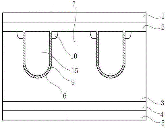
[0065]The remaining steps in the manufacturing method of trench Schottky barrier diodes in this embodiment are the same as those in Embodiment 1, except that the doping method of the conductive polysilicon 8 and the corner protection region 10 in step (9) is different. Step (nine) of the embodiment is: as Figure 9 As shown, the doped glass layer 13 is firstly deposited on the exposed corner top surface of the boss 7 and the top surface of the polysilicon 15 by high-temperature diffusion method, and after thermal annealing, the doped glass layer 13 is selectively removed by wet etching to form Conductive polysilicon 8, and at the same time form corner protection regions 10.


PUM

PropertyMeasurementUnit
thicknessaaaaaaaaaa
thicknessaaaaaaaaaa
thicknessaaaaaaaaaa

Abstract

The invention discloses a trenched Schottky-barrier diode, and solves the problems that a conventional trenched Schottky-barrier diode is lower in performance and reliability, high in reverse current leakage and poor in reverse blocking capability. The doping density of an epilayer gradually increases from the top to bottom, a second conduction type non-uniformly doped conductive polycrystalline silicon of which the doping density gradually decreases from the top to bottom is filled in trenches, second conduction type heavily doped lug boss apex angle protection areas are formed at the apex angles on two sides of lug bosses, and a Schottky-barrier metal layer in ohmic contact with the top surfaces of both the conductive polycrystalline silicon and the lug boss apex angle protection areas is added to the bottom surface of an anodal metal layer. The trenched Schottky-barrier diode provided by the invention has the advantages of low reverse current leakage, good voltage reverse blocking capability and excellent reliability. The invention also provides a manufacturing method of the trenched Schottky-barrier diode, which has the advantages of less steps and low manufacturing cost and can effectively isolate areas from damage by the technological process and contamination of impurities due to local impairment of isolating layers.

Description

technical field [0001] The invention relates to the technical field of semiconductors, in particular to a trench Schottky barrier diode and a manufacturing method thereof. Background technique [0002] As a conversion device from AC to DC, the rectifier device requires unidirectional conduction characteristics, that is, low turn-on voltage and small on-resistance during forward conduction, and high blocking voltage and low reverse leakage when reverse biased. Schottky barrier diodes have been used in power supply applications for decades as rectifier devices. Due to their advantages of low forward turn-on voltage and fast switching speed, they are very suitable for switching power supplies and high-frequency applications. [0003] Schottky barrier diodes are manufactured using the principle of a metal-semiconductor junction formed by contact between a metal and a semiconductor. Traditional planar Schottky barrier diode devices are usually composed of a low doping concentrat...

Claims


Application Information

Patent Timeline
Patent Type & Authority Applications(China)
IPC IPC(8): H01L29/872H01L21/329
CPCH01L29/8725H01L29/66143
Inventor 刘伟
Owner HANGZHOU LION MICROELECTRONICS CO LTD
Why Eureka
Try Eureka