Nano doping structure and preparation method thereof

A nanostructure and nanotechnology, applied in the direction of nanotechnology, nanotechnology, nanotechnology for materials and surface science, etc., can solve problems such as inability to dope nanomaterials, difficulty in doping measurement, and shape change of nanomaterials, to achieve Wide range of applications, precise control of doping metering, and precise control of thickness

Active Publication Date: 2015-03-04
青岛艾斯达特新材料科技有限公司
View PDF4 Cites 0 Cited by
  • Summary
  • Abstract
  • Description
  • Claims
  • Application Information

AI Technical Summary

Problems solved by technology

For example, the most widely used in-situ doping method is to add dopant substances to the precursor during the growth stage of the nanowires. The self-cleaning of crystalline nanomaterials and the physical and chemical properties of doped materials make this method difficult to control the doping metering, and the shape of nanomaterials changes after doping, which ultimately reduces the doping effect.
In addition, the thermal diffusion method is also a commonly used nanomaterial doping method, but due to high temperature, it cannot be applied to low melting point materials, and there are also defects similar to in-situ doping
Due to the complex morphology of nanomaterials, ion implantation cannot uniformly dope nanomaterials well.

Method used


Image

  • Nano doping structure and preparation method thereof
  • Nano doping structure and preparation method thereof
  • Nano doping structure and preparation method thereof

Examples


Embodiment Construction

[0027] The present invention will be further described below in conjunction with drawings and embodiments.

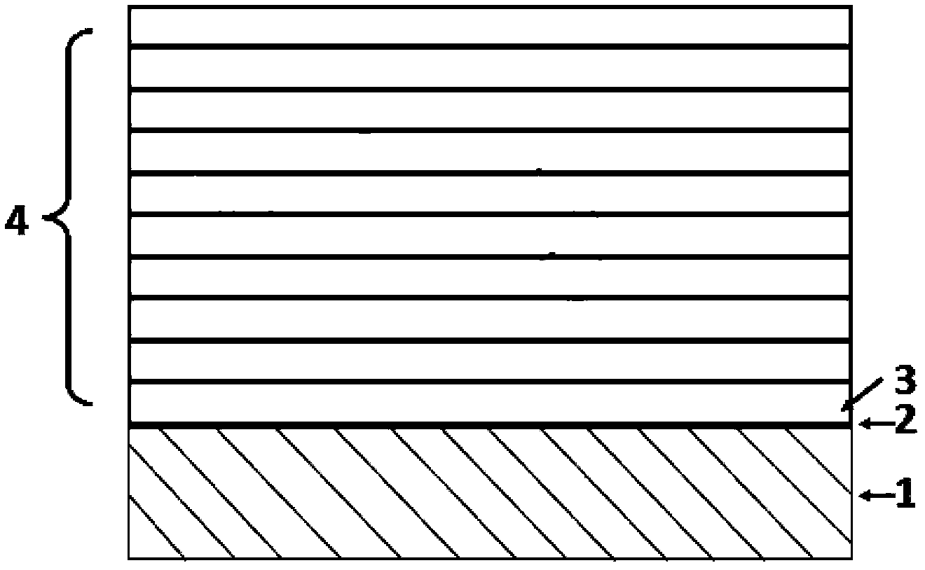
[0028] The invention provides a method for doping nanometer materials by atomic layer deposition technology. The atomic layer deposition system consists of a reaction chamber, a vacuum system, a heating system and a precursor control system. Taking Al-doped ZnO nanowires as an example to illustrate the specific implementation method.

[0029] see figure 1 , the specific process is:

[0030] 1) Put the pre-grown ZnO nanowires (substrate) into the reaction chamber of the atomic layer deposition system, evacuate to the ultimate vacuum, and then pass the flushing inert gas N 2 , keep the background air pressure at 260-300 mTorr, and the reaction chamber temperature at 150°C;

[0031] 2) First deposit a cycle of Al on the nanowire substrate 2 o 3 , In the reaction chamber of the atomic layer deposition system, high-purity nitrogen is used as the carrier gas and flushin...


PUM


Abstract

The invention provides a nano doping structure and a preparation method thereof. The preparation method comprises the following steps of: 1) placing a nano material into a reaction chamber of an atom layer depositing system; 2) utilizing an atom layer depositing method to deposit a dopant material with the thickness of 1-2 cycles; 3) depositing a base material of a nano material with the thickness of X cycles; and 4) alternatively and circularly depositing dopants and substrate material layers obtained in the steps 2) and 3) with the thickness of Y cycles, wherein the selection of the X is determined according to an actual doping ratio; when the X is smaller, a doping ratio is larger; and the selection of the Y is determined according to the thickness of an actually-needed doping layer, and the doping layer is thicker when the Y is greater. According to the nano doping structure and the preparation method thereof, an in-situ atom layer depositing technology is adopted, a process is simple and is easy to realize, a reaction temperature is low and an applicable material range is wide.

Description

technical field [0001] The invention belongs to the technical field of semiconductor manufacturing and doping, and in particular relates to a method for doping nanometer materials by atomic layer deposition technology. Background technique [0002] The 21st century is the century of information and nanoscience. Nanotechnology plays an increasingly important role in the fields of light, electricity, heat, magnetism, sound, and machinery. Nanotechnology will surely lead the development of science and technology in the 21st century, and nanotechnology has advanced to the practical stage at this stage. [0003] Trace element doping is an important means to control the physical and chemical properties of materials. For example, doping a small amount of P or B on traditional bulk semiconductor Si-based materials can realize the regulation of its P or N type. By controlling the doping amount, it can be significantly adjusted. Conductivity. The doping methods for traditional bulk ...

Claims


Application Information

Patent Timeline
Patent Type & Authority Patents(China)
IPC IPC(8): C23C16/44B82Y30/00B82Y40/00
Inventor 马大衍王红波马飞徐可为
Owner 青岛艾斯达特新材料科技有限公司
Why Eureka
Try Eureka