NiO/GaN p-n junction-based self-powered ultraviolet detector and preparation method thereof
An ultraviolet detector, p-nio technology, applied in the field of photoelectric detectors, can solve the problems of slow response speed, unfavorable development trend, increasing the size of the detector, etc., to achieve less impurities, strong process controllability, stable and uniform thickness Effect
- Summary
- Abstract
- Description
- Claims
- Application Information
AI Technical Summary
Problems solved by technology
Method used
Image
Examples
Embodiment 1
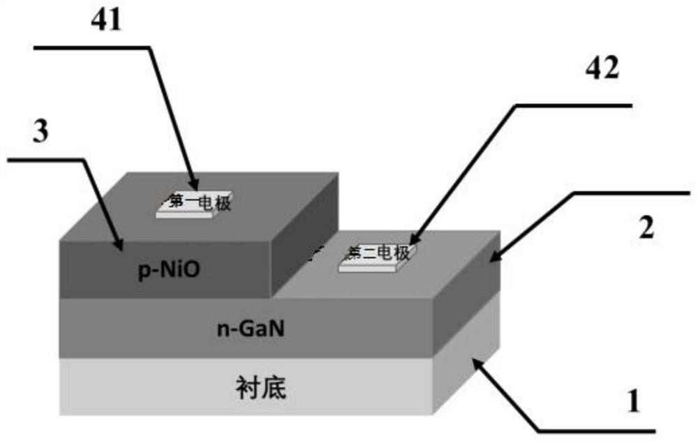
[0025] A method for preparing a self-powered ultraviolet detector based on a NiO / GaN p-n junction comprises the following steps:
[0026] The n-GaN layer is grown on the substrate by metal-organic chemical vapor deposition;
[0027] growing a p-NiO layer by magnetron sputtering on the side of the GaN layer away from the substrate;
[0028] A metal electrode is vapor-deposited on the n-GaN layer and the p-NiO layer by thermal evaporation, that is, the second electrode on the n-GaN layer and the first electrode on the p-NiO layer are formed. electrode.
[0029] The preparation process of the embodiment of the present application is simple, the process is highly controllable, and easy to operate. The surface of the n-GaN layer prepared by the method of metal-organic chemical vapor deposition and the p-NiO layer grown by magnetron sputtering are dense and thick. It is stable and uniform, can be prepared in a large area, and has good repeatability.
[0030] For the convenience o...
Embodiment 2
[0041] The difference from the variant embodiment 1 is that the substrate of the embodiment of the present application is a copper mesh substrate. Specifically, the method for preparing a self-powered ultraviolet detector based on a NiO / GaN p-n junction according to the embodiment of the present application specifically includes the following steps:
[0042] (1) Divide 10×10mm 2 The large and small copper grids were ultrasonically cleaned with acetone, absolute ethanol, and deionized water for 15 minutes, and then high-purity N 2 Pretreatment such as drying is performed to obtain a pretreated substrate.
[0043] (2) Put the dried copper mesh substrate into the metal-organic chemical vapor deposition MOCVD reaction chamber, and then 3 Under the atmosphere, using metal gallium as the gallium source, the temperature was raised to 800°C, and the copper grid substrate was nitrided, and then lowered to 600°C to grow n-GaN thin films, NH 3 The flow rate is 100mL / min, the metal-org...
Embodiment 3
[0052] The difference from Example 1 lies in the electrode fabrication in step (4), the first electrode and the second electrode in the example of the present application are graphene electrodes.
[0053] Specifically, the method for preparing a self-powered ultraviolet detector based on a NiO / GaN p-n junction according to the embodiment of the present application specifically includes the following steps:
[0054] (1) Divide 10×10mm 2 The large and small copper grids were ultrasonically cleaned with acetone, absolute ethanol, and deionized water for 15 minutes, and then high-purity N 2 Pretreatment such as drying is performed to obtain a pretreated substrate.
[0055] (2) Put the dried copper mesh substrate into the metal-organic chemical vapor deposition MOCVD reaction chamber, and then 3 Under the atmosphere, using metal gallium as the gallium source, the temperature was raised to 800°C, and the copper grid substrate was nitrided, and then lowered to 600°C to grow n-GaN t...
PUM
| Property | Measurement | Unit |
|---|---|---|
| thickness | aaaaa | aaaaa |
| thickness | aaaaa | aaaaa |
| thickness | aaaaa | aaaaa |
Abstract
Description
Claims
Application Information


