Method for growing germanium-silicon epitaxial layers

A silicon germanium epitaxy and epitaxial growth technology, which is applied in the direction of electrical components, semiconductor/solid-state device manufacturing, circuits, etc., can solve the problems of SiGe epitaxial layer critical thickness reduction, SiGe epitaxial layer surface roughness, etc., to improve rough surface morphology, Reduce the effect of strain relaxation

Inactive Publication Date: 2013-03-06
SEMICON MFG INT (SHANGHAI) CORP
View PDF6 Cites 17 Cited by
  • Summary
  • Abstract
  • Description
  • Claims
  • Application Information

AI Technical Summary

Problems solved by technology

[0020] In view of this, the technical problem solved by the present invention is: the increase of Ge content in the SiGe epitaxial layer above the PMOS source and drain

Method used


Image

  • Method for growing germanium-silicon epitaxial layers
  • Method for growing germanium-silicon epitaxial layers
  • Method for growing germanium-silicon epitaxial layers

Examples


specific Embodiment 1

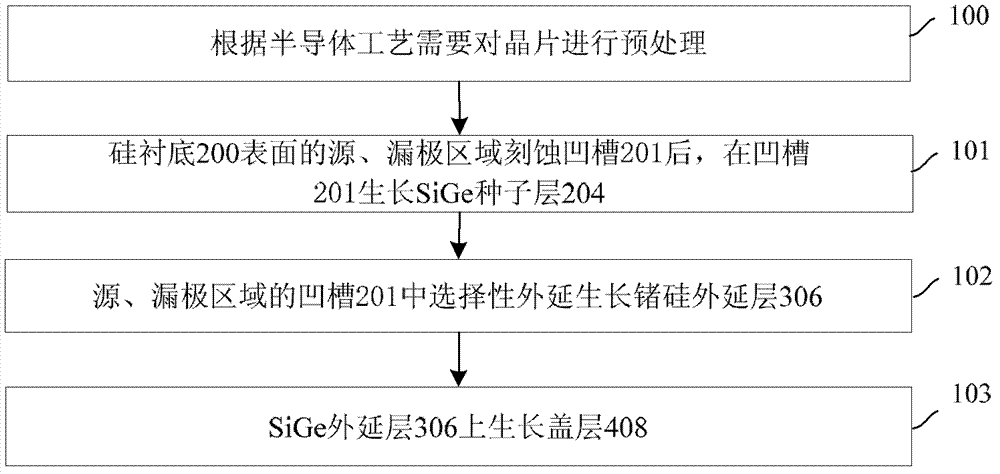
[0040] Combine below Figure 6-8 The process flow of the present invention for epitaxially growing a carbon-containing SiGe epitaxial layer will be described in detail.

[0041] Step 500, performing pretreatment on the wafer according to the requirements of the semiconductor process;

[0042] In this step, the pretreatment of the wafer includes removing the oxide layer and impurities on the surface of the silicon substrate. For a heavily doped silicon substrate, it must be considered whether a backseal is required to reduce the self-sufficiency in the subsequent selective epitaxial growth process. doping phenomenon.

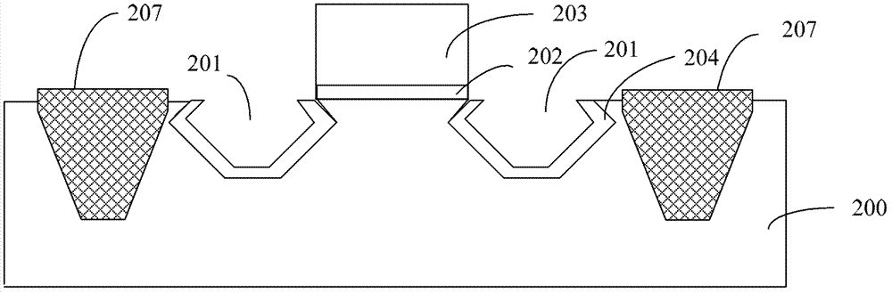
[0043] Step 501, after etching the groove 201 in the source and drain regions on the surface of the silicon substrate 200, grow a SiGe seed layer 204 on the surface of the groove 201 to form a Image 6 The schematic diagram of the cross-sectional structure shown;

[0044] In this step, if Image 6 As shown, the active regions are isolated by STI207, and the s...


PUM


Abstract

The invention provides a method for epitaxially growing SiGe epitaxial layers. The method is applied to filling the SiGe epitaxial layers in source and drain electrode regions of a PMOS (P-channel metal oxide semiconductor), and reaction gas containing Ge elements and carbonaceous gas are simultaneously filled into a reaction chamber, so that the carbonaceous SiGe epitaxial layers are selectively and epitaxially grown on surfaces of source and drain electrode regions of the surface of a silicon substrate. The method has the advantages that on the premise that contents of Ge elements in the SiGe epitaxial layers are guaranteed, critical thicknesses of the SiGe epitaxial layers are increased, strain relaxation is avoided, and the carrier mobility of the PMOS is improved.

Description

technical field [0001] The invention relates to a semiconductor manufacturing method, in particular to a silicon germanium epitaxial layer growth method. Background technique [0002] At present, the semiconductor manufacturing industry mainly grows devices on the wafer (wafer) device surface of the silicon substrate. For example, the metal-oxide semiconductor field effect transistor (Metal-Oxide Semiconductor Field Effect Transistor, MOSFET) device structure includes an active region, a source , a drain and a gate, wherein the active region is located in the semiconductor silicon substrate, the gate is located above the active region, and ion implantation is performed in the active regions on both sides of the gate to form a source and a drain There is a conductive channel under the gate, and there is a gate dielectric layer between the gate and the conductive channel. According to different types of ion implantation, hole type metal oxide semiconductor field effect transi...

Claims


Application Information

Patent Timeline
IPC IPC(8): H01L21/20H01L21/336
Inventor 涂火金
Owner SEMICON MFG INT (SHANGHAI) CORP
Why Eureka
Try Eureka