Production method of interconnection structure with materials containing polymer and metal through holes

A polymer material and manufacturing method technology, applied in semiconductor/solid-state device manufacturing, electrical components, circuits, etc., can solve the problems of high cost, complicated steps, and long time, and achieve low cost, few manufacturing steps, and simple processing flow Effect

Inactive Publication Date: 2013-03-06
INST OF MICROELECTRONICS CHINESE ACAD OF SCI
View PDF9 Cites 11 Cited by
  • Summary
  • Abstract
  • Description
  • Claims
  • Application Information

AI Technical Summary

Problems solved by technology

[0007] One of the purposes of the present invention is to provide a method for manufacturing an interconnection structure containing polymer materials and metal vias that overcomes the problems of voids, complicated steps, long time, and high cost in the metal filling process

Method used


Image

  • Production method of interconnection structure with materials containing polymer and metal through holes
  • Production method of interconnection structure with materials containing polymer and metal through holes
  • Production method of interconnection structure with materials containing polymer and metal through holes

Examples


Embodiment Construction

[0031] A method for manufacturing an interconnection structure containing a polymer material and a metal via provided in an embodiment of the present invention includes:

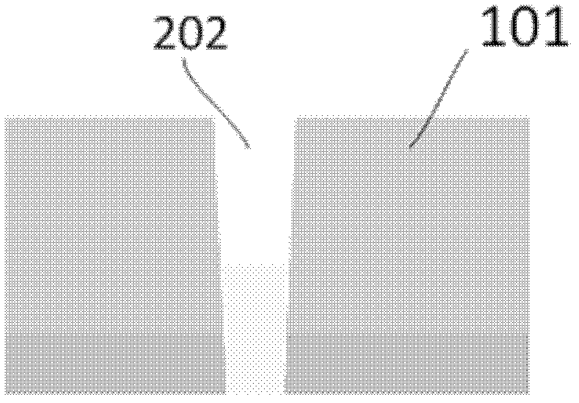
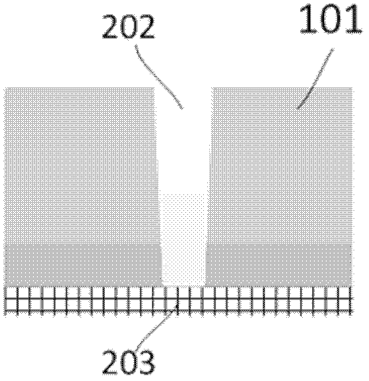
[0032] Step S1, making blind holes or through holes on the substrate. Substrates include glass substrates, silicon wafers, and other semiconductor substrates. Blind or through holes are made using laser drilling, dry etching, sandblasting or mechanical methods.

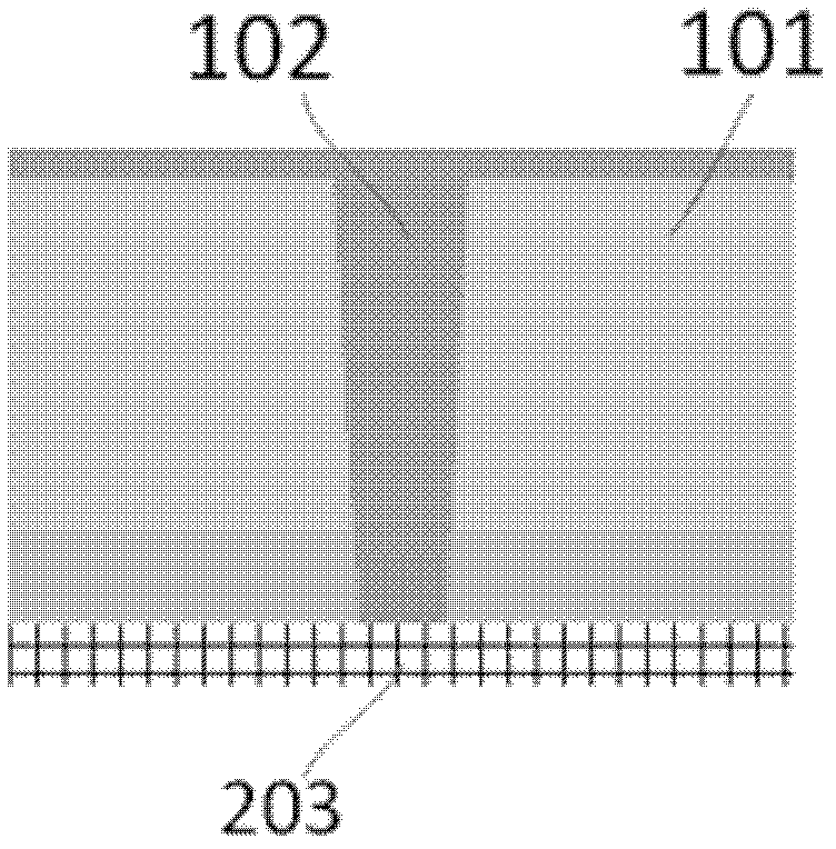
[0033] Step S2, filling polymer in the blind hole or through hole. Polymer filling is achieved by spin-coating method. Polymers include benzocyclobutene or epoxy based resins.

[0034] Step S3, inserting the metal block into the blind hole or through hole filled with polymer. An auxiliary film is attached to the bottom of the substrate before filling the via holes with polymer. When the metal block is inserted, the polymer in the blind hole or through hole is in a liquid or semi-cured state. Metal blocks include nickel, iron, copper, aluminum,...


PUM


Abstract

The invention discloses a production method of an interconnection structure with materials containing polymer and metal through holes. The production method includes: reserving blind holes or through holes on a substrate, and filling polymer in the blind holes or through holes; inserting metal blocks into the blind holes or through holes filled with polymer; solidifying polymer in the blind holes or the through holes; and grinding and polishing the front and the back of the substrate to expose the metal. By the production method, the multilayer stack structure adopted in three-dimensional packaging or MEMS (micro-electro-mechanical systems) packaging can be achieved effectively.

Description

technical field [0001] The invention relates to the technical field of microelectronic packaging, in particular to a method for manufacturing an interconnection structure containing polymer materials and metal vias. Background technique [0002] With people's requirements for the development of electronic products in the direction of miniaturization, high performance, and multi-function, researchers strive to make electronic systems smaller and smaller, with stronger performance and more functions. Many new technologies, new materials and new designs, among which three-dimensional packaging technology and system-in-package (System-in-Package, SiP) technology are typical representatives of these technologies. [0003] Three-dimensional packaging technology refers to the packaging technology that stacks two or more chips in the same package in the vertical direction without changing the size of the package. Interposer technology is one of the key technologies to realize thre...

Claims


Application Information

Patent Timeline
Patent Type & Authority Applications(China)
IPC IPC(8): H01L21/768
Inventor 于大全赫然孙瑜
Owner INST OF MICROELECTRONICS CHINESE ACAD OF SCI
Why Eureka
Try Eureka