Double-conduction semiconductor component and manufacturing method thereof

A manufacturing method and semiconductor technology, applied in the direction of semiconductor devices, semiconductor/solid-state device manufacturing, transistors, etc., can solve problems such as poor withstand voltage capability and increased manufacturing cost, achieve improved withstand voltage capability, and reduce the size of double-conduction semiconductor components Effect

Inactive Publication Date: 2013-03-06
SINOPOWER SEMICON
View PDF6 Cites 1 Cited by
  • Summary
  • Abstract
  • Description
  • Claims
  • Application Information

AI Technical Summary

Problems solved by technology

In this way, the withstand voltage capability of the N-type epitaxial layer 14 can be improved. However, the provided P-type substrate 12 and the N-type epitaxial layer 14 have different conductivity types, so an additional epitaxial process is required to form on the P-type substrate 12. N-type epitaxial layer 14, while increasing production cost
Therefore, at present, there are also developments to manufacture double-conduction semiconductor components on N-type substrates, but the double-conduction semiconductor components produced have poor withstand voltage capability.

Method used


Image

  • Double-conduction semiconductor component and manufacturing method thereof
  • Double-conduction semiconductor component and manufacturing method thereof
  • Double-conduction semiconductor component and manufacturing method thereof

Examples


Embodiment Construction

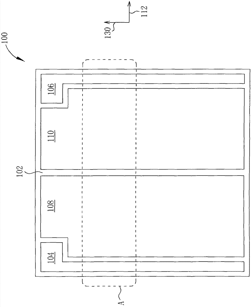
[0042] Please refer to figure 2 , figure 2 It is a schematic top view of a double conduction semiconductor device according to a preferred embodiment of the present invention. like figure 2 As shown, the double conduction semiconductor device 100 includes a semiconductor substrate 102, a first gate metal layer 104, a second gate metal layer 106, a first source metal layer 108 and a second source metal layer 110 . The first gate metal layer 104 , the first source metal layer 108 , the second source metal layer 110 and the second gate metal layer 106 are disposed on the semiconductor substrate 102 and arranged in sequence along a first direction 112 . The first gate metal layer 104 and the first source metal layer 108 are used to electrically connect the gate and the source of a first MOSFET in the dual-conduction semiconductor device 100 to the outside respectively, and the second The two gate metal layers 106 and the second source metal layer 110 are used to electricall...


PUM


Abstract

The invention discloses a double-conduction semiconductor component. The double-conduction semiconductor component comprises a semiconductor substrate, a first substrate doping area, a second substrate doping area and a grid insulation layer, wherein the semiconductor substrate is provided with a first conduction type, and both the first substrate doping area and the second substrate doping area are provided with second conduction types. The semiconductor substrate is provided with a first groove, the first substrate doping area and the second substrate doping area are respectively arranged in the semiconductor substrate on two sides of the first groove, the grid insulation layer covers the surface of the first groove and is provided with a first part, a second part and a third part, wherein the first part is adjacent to the first substrate doping area, the second part is adjacent to the second substrate doping area, and the third part is arranged at a turning position of the bottom and the side wall of the first groove. The thickness of each of the first part and the second part is smaller than that of the third part. Therefore, withstand voltage of the double-conduction semiconductor component can be increased.

Description

technical field [0001] The invention relates to a double conduction semiconductor component and a manufacturing method thereof, in particular to a double conduction semiconductor component and a manufacturing method thereof, the bottom thickness of the gate insulating layer is greater than the side wall thickness. Background technique [0002] A conventional bilateral conduction semiconductor device is installed in a battery and is used to protect the battery from damage due to charging and discharging during the charging and discharging process of the battery. In order to have the effect of protecting the battery, the known dual-conduction semiconductor component is composed of two N-type power MOSFETs (MOSFETs), and the drains of the two N-type power MOSFETs are electrically connected to Together. Moreover, each N-type power metal oxide semiconductor field effect transistor has a parasitic diode (diode), and the P terminal of the diode is electrically connected to the sou...

Claims


Application Information

Patent Timeline
Patent Type & Authority Applications(China)
IPC IPC(8): H01L27/088H01L29/78H01L29/423H01L21/8234
CPCH01L29/41766H01L29/66734H01L29/66719H01L29/66727H01L29/42368H01L29/7813H01L29/7831
Inventor 林伟捷
Owner SINOPOWER SEMICON
Why Eureka
Try Eureka