Planar gate IGBT (Insulated Gate Bipolar Transistor) chip

A planar gate and chip technology, applied in electrical components, circuits, semiconductor devices, etc., can solve problems such as planar gate IGBT structure, single hole blocking effect, etc., to enhance conductance modulation effect and improve electron injection efficiency , The effect of optimizing the conduction voltage drop

Active Publication Date: 2013-03-13
ZHUZHOU CRRC TIMES SEMICON CO LTD
View PDF9 Cites 10 Cited by
  • Summary
  • Abstract
  • Description
  • Claims
  • Application Information

AI Technical Summary

Problems solved by technology

But the patent is only for trench gate IGBT, not mentioning planar gate IGBT structure
In addition, the patent does not involve N-type carrier buried layer structure
[0008] The various existing technologies mentioned above have enhanced the conductance modulation effect of the IGBT to a certain extent, thereby reducing the conduction voltage drop, but these solutions only have a single hole blocking effect (only a barrier blocking effect)
The aforementioned patent proposes a method with physical barrier effect, but only limited to trench gate IGBT

Method used


Image

  • Planar gate IGBT (Insulated Gate Bipolar Transistor) chip
  • Planar gate IGBT (Insulated Gate Bipolar Transistor) chip
  • Planar gate IGBT (Insulated Gate Bipolar Transistor) chip

Examples


Embodiment Construction

[0069] The following will clearly and completely describe the technical solutions in the embodiments of the present invention with reference to the accompanying drawings in the embodiments of the present invention. Obviously, the described embodiments are only part of the embodiments of the present invention, not all of them. Based on the embodiments of the present invention, all other embodiments obtained by persons of ordinary skill in the art without creative efforts fall within the protection scope of the present invention.

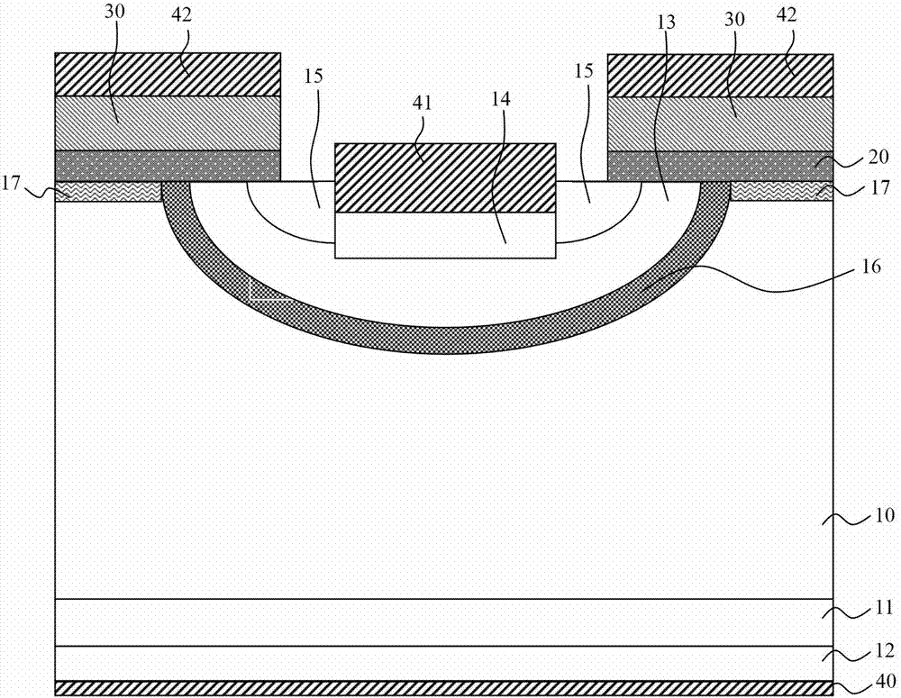
[0070] as attached figure 2 to attach Figure 15 As shown, a specific embodiment of a planar gate IGBT chip of the present invention is given, and the present invention will be further described below in conjunction with the accompanying drawings and specific embodiments.

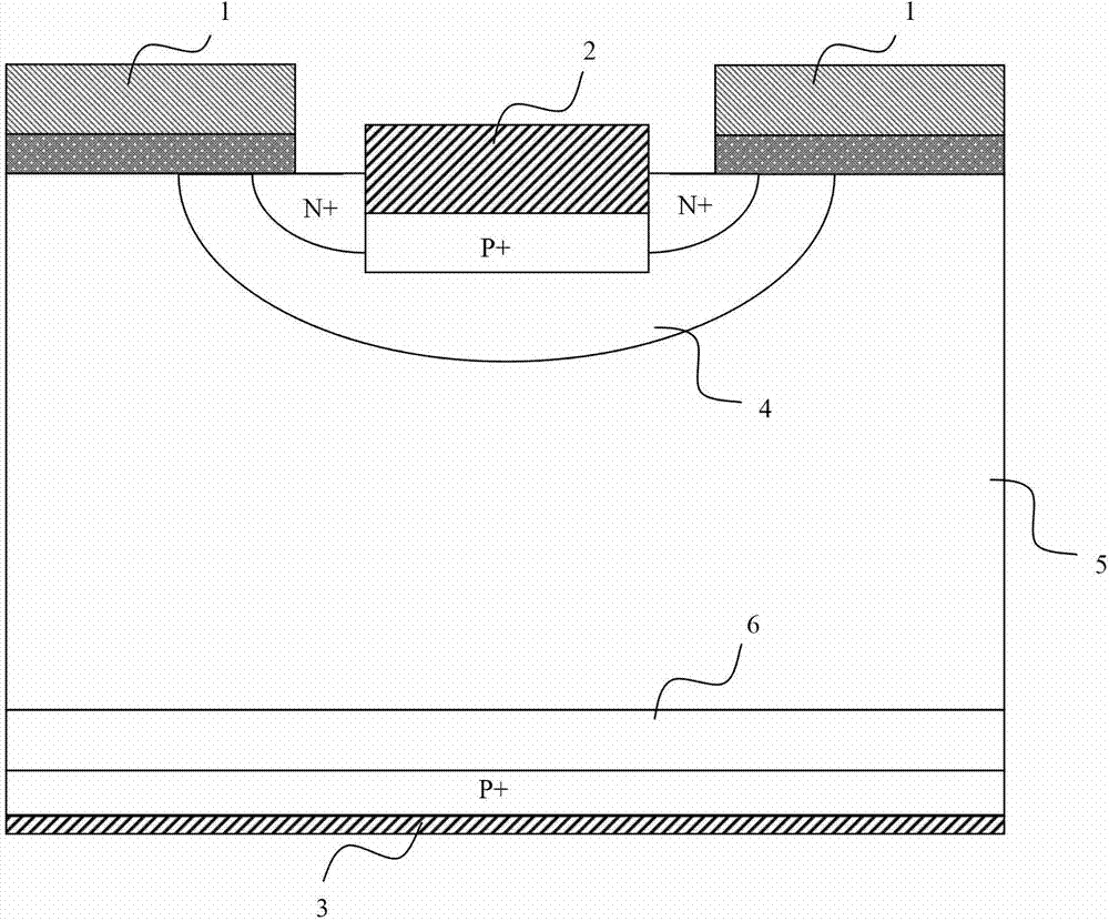
[0071] as attached Figure 7 Shown is a schematic cross-sectional structure diagram of a single cell in a specific embodiment of the planar gate IGBT chip of the present inventi...


PUM


Abstract

The invention discloses a planar gate IGBT (Insulated Gate Bipolar Transistor) chip, which comprises a collector metal electrode, a P+ collector region, an N- drift region, a P- base region, a P+ ohmic contact region, an N+ source region, a gate oxide layer, a polysilicon gate and a gate metal electrode which are arranged successively, and an emitter metal electrode arranged above the P+ ohmic contact region, wherein the polysilicon gate of the planar gate IGBT chip adopts a planar gate structure. The planar gate IGBT chip also comprises a first N-type carrier buried layer and/or a second N-type carrier buried layer. The first N-type carrier buried layer is located below the P- base region. The second N-type carrier buried layer is located below the gate oxide layer and at both sides of the P- base region. The planar gate IGBT chip has the beneficial effects that the compromise relation between conduction pressure drop and turn-off loss of the IGBT is reduced, lower power consumption is realized, and thus the power density, the operating junction temperature and the long-term reliability of the IGBT chip are increased.

Description

technical field [0001] The invention relates to a semiconductor IGBT (Insulted Gate Bipolar Transistor, insulated gate bipolar transistor) chip structure, in particular to a planar gate IGBT chip structure with double hole blocking effect. Background technique [0002] Insulated gate bipolar transistor (IGBT) has the characteristics of on-state voltage drop, large current capacity, high input impedance, fast response and simple control, and is widely used in industry, information, new energy, medicine, transportation, military and aviation fields . as attached figure 1 Shown is a schematic structural diagram of a conventional planar gate IGBT, which includes a gate 1 , an emitter 2 , a collector 3 , a P-well 4 , an N drift region 5 and an N buffer region 6 . In order to reduce the turn-on voltage drop of the IGBT, a trench gate structure is used. However, after trench etching, the surface is rough and the damage is large, which will affect the mobility of carriers; the ro...

Claims


Application Information

Patent Timeline
Patent Type & Authority Applications(China)
IPC IPC(8): H01L29/739H01L29/06
CPCH01L29/0649H01L29/0696H01L29/7396
Inventor 刘国友覃荣震黄建伟
Owner ZHUZHOU CRRC TIMES SEMICON CO LTD
Why Eureka
Try Eureka