High-voltage device in composite structure and starting circuit

A high-voltage device and high-voltage technology, applied in the field of high-voltage devices and start-up circuits, can solve the problems of increased chip cost and large chip area, and achieve the effects of improving conversion efficiency, saving circuit components, and reducing difficulty

Active Publication Date: 2013-03-27
SHENZHEN SUNMOON MICROELECTRONICS
View PDF3 Cites 23 Cited by
  • Summary
  • Abstract
  • Description
  • Claims
  • Application Information

AI Technical Summary

Problems solved by technology

In the power supply chip that also integrates high-voltage power MOS inside the controller chip, the problem is more prominent, and the chip area is large, resulting in an increase in chip cost

Method used


Image

  • High-voltage device in composite structure and starting circuit
  • High-voltage device in composite structure and starting circuit
  • High-voltage device in composite structure and starting circuit

Examples


Embodiment Construction

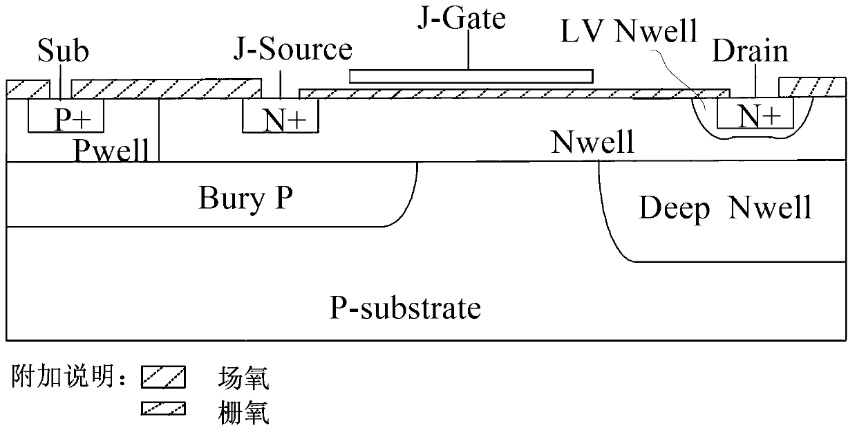
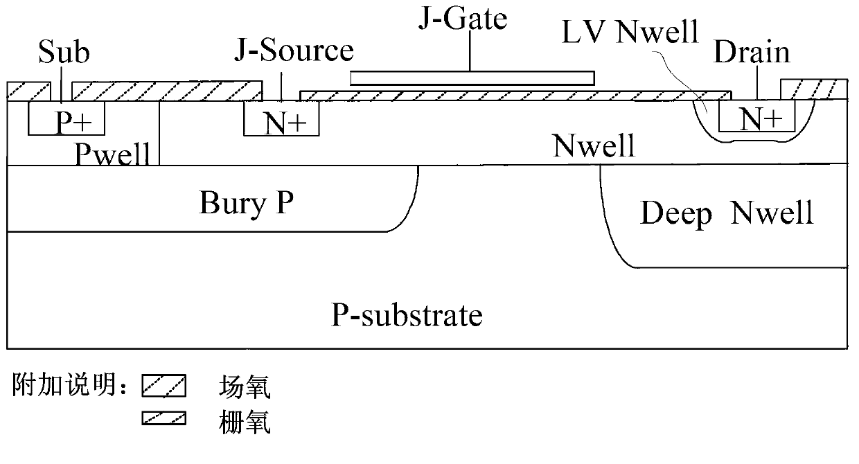
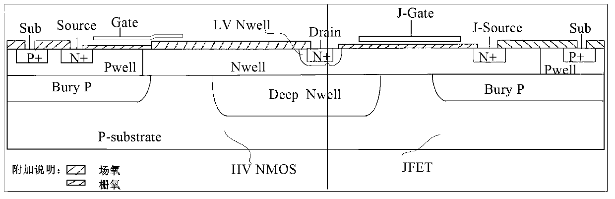
[0027] Embodiments of the present invention are described in detail below, examples of which are shown in the drawings, wherein the same or similar reference numerals designate the same or similar elements or elements having the same or similar functions throughout. The embodiments described below by referring to the figures are exemplary only for explaining the present invention and should not be construed as limiting the present invention.

[0028] P-substrate in the text and attached drawings means P-type substrate layer, Pwell means P-type well region; Bury P means P-type buried layer; Deep Nwell means deep N-type well region; Nwell means N-type well region; LV Nwell means low voltage N-type well region; P+ indicates P-type high-concentration implantation, N+ indicates N-type high-concentration implantation, Sub indicates the substrate connection terminal, Source indicates the source terminal of the device, Drain indicates the drain terminal of the device, and Gate indicate...


PUM


Abstract

An embodiment of the invention provides a high-voltage device in a composite structure. The high-voltage device in the composite structure comprises a high-voltage power tube HVNMOS and a JFET tube. The high-voltage power tube HVNMOS comprises a drain electrode, a source electrode, a grid electrode and a substrate, and a P-type well region P well arranged between the source electrode and the drain electrode is adopted as a conducting channel. The JFET tube comprises a drain electrode, a source electrode, a grid electrode and a substrate, and an N-type well region N well arranged between the source electrode and the drain electrode is adopted as a conducting channel. The high-voltage power tube HVNMOS and the JFET tube share the same drain electrode, and the N-type double diffusion process is adopted for the drain electrode. A starting circuit provided with the high-voltage device in the composite structure is further provided. By adopting the high-voltage device in the composite structure, chip area is effectively saved and chip cost is reduced.

Description

technical field [0001] The invention relates to the technical field of semiconductor devices, in particular, the invention relates to a high-voltage device and a starting circuit of a composite structure. Background technique [0002] In the application field of AC / DC switching power supply, the controller chip needs a start-up circuit to provide it with the voltage required to turn it on. In traditional applications, the start-up circuit is to connect a large resistor in series from the output end of the rectifier bridge to the power supply end of the controller. The output terminal of the rectifier bridge charges the bypass capacitor of the controller chip through a large resistor. When it reaches the starting voltage, the controller starts and the system starts to work normally. After the start-up is completed, the energy required by the power supply is mainly supplied to the controller chip by the auxiliary winding. After the controller chip works normally, the resistan...

Claims


Application Information

Patent Timeline
Patent Type & Authority Applications(China)
IPC IPC(8): H01L27/02H01L27/088H01L27/098H02M1/36
CPCH03K17/22H01L29/7835H01L29/808H01L29/7832H01L27/098H03K3/353H01L27/088H01L27/0203H01L27/085H02M1/36H01L29/0623H01L29/7817
Inventor 李照华林道明赵春波胡乔戴文芳
Owner SHENZHEN SUNMOON MICROELECTRONICS
Why Eureka
Try Eureka