

Thin film transistor and manufacture method, array substrate and display device thereof
A technology for thin film transistors and manufacturing methods, which is applied in the field of thin film transistor manufacturing, and can solve the problems of reduced lifespan, unstable driving voltage, and poor film-forming quality, and achieve improved stability and life, good surface appearance, and film-forming quality Good results
- Summary
- Abstract
- Description
- Claims
- Application Information
AI Technical Summary
Problems solved by technology
Method used
Image

Examples
Embodiment Construction
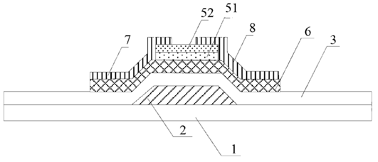
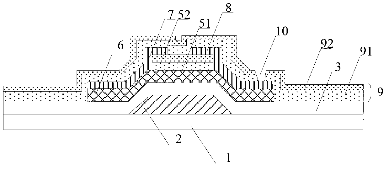
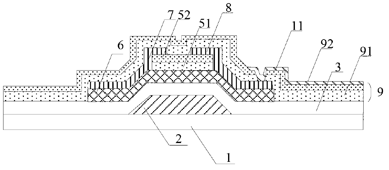
[0058] Embodiments of the present invention provide a thin film transistor and its manufacturing method, an array substrate and a display device, which are used to improve the stability of the driving voltage of the thin film transistor and the lifespan of the thin film transistor.
[0059] In an embodiment of the present invention, an insulating layer in contact with the active layer is formed on the substrate on which the active layer is formed. At least two insulating layers are used. It is made under high temperature conditions, and the other insulating layers except the one closest to the active layer are made under high temperature conditions of 300°C-400°C. The insulation layer made under low temperature conditions has a better contact interface quality with the active layer, and the formed surface morphology is better, which is conducive to the formation of a TFT with higher stability and performance. The insulating layer made under high temperature conditions has a ve...
PUM
 Abstract
Description
Claims
Application Information