Processing Method and Recording Medium

Inactive Publication Date: 2010-08-26
TOKYO ELECTRON LTD
View PDF5 Cites 2 Cited by
  • Summary
  • Abstract
  • Description
  • Claims
  • Application Information

AI Technical Summary

Benefits of technology

[0007]The present invention was made in view of the above problems, and its object is to provide a processing method capable of removing an oxide film adhering to a Si layer from the Si layer without adversely affecting parts other than the oxide film and capable of surely forming a SiGe layer with good film quality without roughening the crystal structure of a surface of the Si layer from which the oxide film has been removed, and to provide a recording medium.Means for Solving the Problems
[0015]According to the present invention, it is possible to remove an oxide film from a Si layer without adversely affecting parts other than the oxide film and to surely form a SiGe layer with good film quality on the Si layer without roughening the crystal structure on a surface of the Si layer from which the oxide film has been removed.

Problems solved by technology

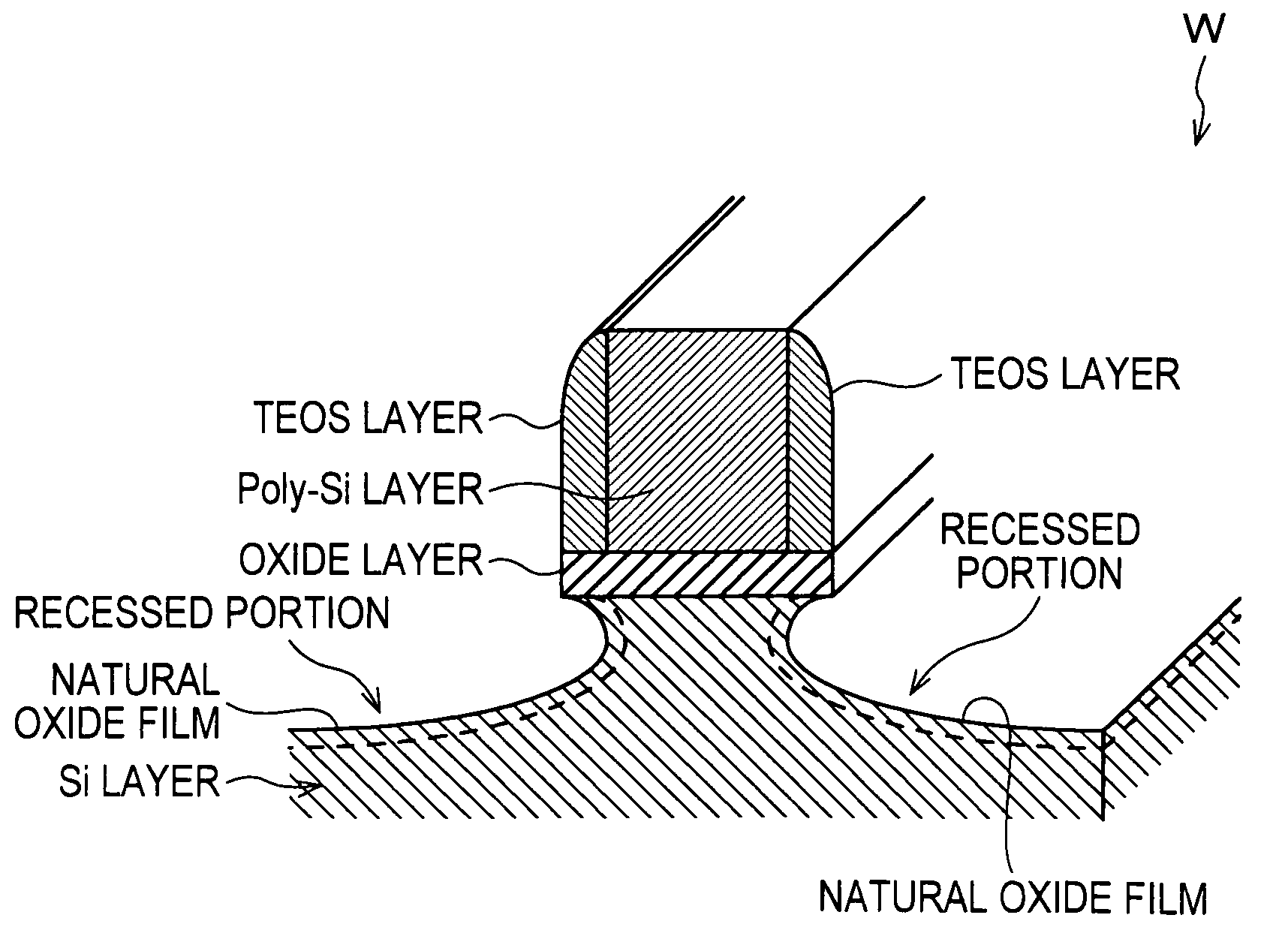
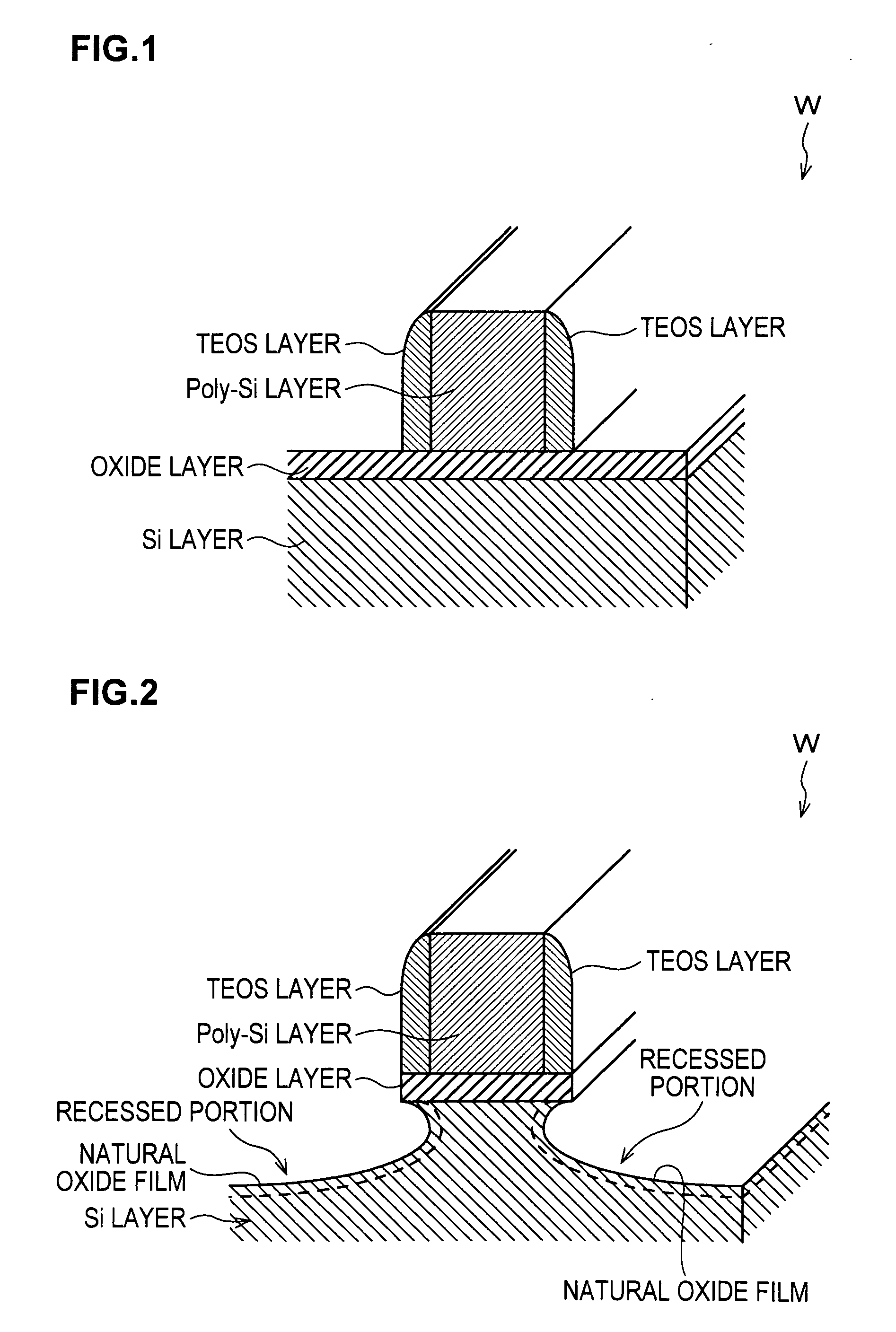
On the surface of the Si layer exposed to the outside air, a natural oxide film (SiO2) easily grows, and the presence of the natural oxide film poses a problem of obstructing the formation of the SiGe layer.

Method used


Image

  • Processing Method and Recording Medium
  • Processing Method and Recording Medium
  • Processing Method and Recording Medium

Examples


example

[0078]The present inventors studied selection ratios as removal amounts regarding various materials used in the manufacture of a semiconductor device when the dry cleaning (etching) including the COR process and the PHT process was performed. FIG. 13 is a graph showing the result of the study. The selection ratio was obtained as a ratio relative to a removal amount of a thermal oxide film (Thermal-Ox) which is defined as 1. The selection ratios of the following six kinds of materials were studied: a polysilazane oxide film (PSZ-SiO2), a thermal CVD oxide film (Thermal-TEOS), a HTO film (Single-HTO), a plasma silicon nitride (plasma-SiN), a thermal CVD nitride film (Thermal-SiN), polysilicon (Poly-Si). As a result, the selection ratios were all 1 or lower. Therefore, it was confirmed that any of the materials is more difficult to chemically react in the COR process than the thermal oxide film (Thermal-Ox) and is not easily damaged by the dry cleaning. That is, it was confirmed that t...


PUM


Abstract

[Object] To provide a processing method capable of removing an oxide film adhering on a Si layer from the Si layer without adversely affecting parts other than the oxide film and capable of surely forming a SiGe layer with good film quality without roughening the crystal structure of a surface of the Si layer from which the oxide film has been removed, and to provide a recording medium.[Means for Solving the Problems] A processing method for removing an oxide film growing on a surface of a Si layer, and forming a SiGe layer on the surface of the exposed Si layer includes: supplying gas containing a halogen element and basic gas to the surface of the Si layer, and causing the oxide film growing on the surface of the Si layer to chemically react with the gas containing the halogen element and the basic gas to turn the oxide film into a reaction product; removing the reaction product by heating; and thereafter forming the SiGe layer on the surface of the exposed Si layer.

Description

TECHNICAL FIELD[0001]The present invention relates to a method of forming a SiGe layer in manufacturing processes of, for example, a semiconductor device.BACKGROUND ART[0002]As a structure of a semiconductor device such as, for example, a transistor, there has been known a structure in which a strained Si layer, an interlayer insulation layer (silicon dioxide (SiO2)), and a gate electrode (polysilicon) are stacked on a surface of a Si (silicon) layer of a semiconductor wafer. Further, a process of forming a SiGe (silicon germanium) crystal layer on the surface of the Si layer is performed (see Patent document 1). Such a SiGe layer is formed by an epitaxial growth reaction, a CVD (Chemical Vapor Deposition) reaction, or the like.[0003]On the surface of the Si layer exposed to the outside air, a natural oxide film (SiO2) easily grows, and the presence of the natural oxide film poses a problem of obstructing the formation of the SiGe layer. Conventionally, the wafer is cleaned by a wet...

Claims


Application Information

Patent Timeline
IPC IPC(8): H01L21/20H01L21/306
CPCH01L21/02057H01L29/165H01L29/7848H01L29/7834H01L29/66636
Inventor MURAKI, YUSUKETOZAWA, SHIGEKIORII, TAKEHIKO
Owner TOKYO ELECTRON LTD
Why Eureka
Try Eureka