Compound semiconductor device and manufacturing method thereof

A manufacturing method, compound technology, applied in semiconductor/solid-state device manufacturing, semiconductor devices, transistors, etc.

Active Publication Date: 2015-12-09
FUJITSU LTD
View PDF12 Cites 0 Cited by
  • Summary
  • Abstract
  • Description
  • Claims
  • Application Information

AI Technical Summary

Problems solved by technology

[0006] However, it is difficult to connect the above-mentioned pn junction diode to a GaN-based HEMT with a vertical structure
In addition, even if you can connect, it will not solve the above problem

Method used


Image

  • Compound semiconductor device and manufacturing method thereof
  • Compound semiconductor device and manufacturing method thereof
  • Compound semiconductor device and manufacturing method thereof

Examples


no. 1 Embodiment approach )

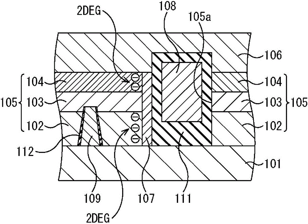
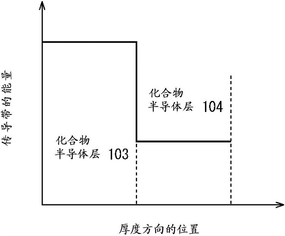
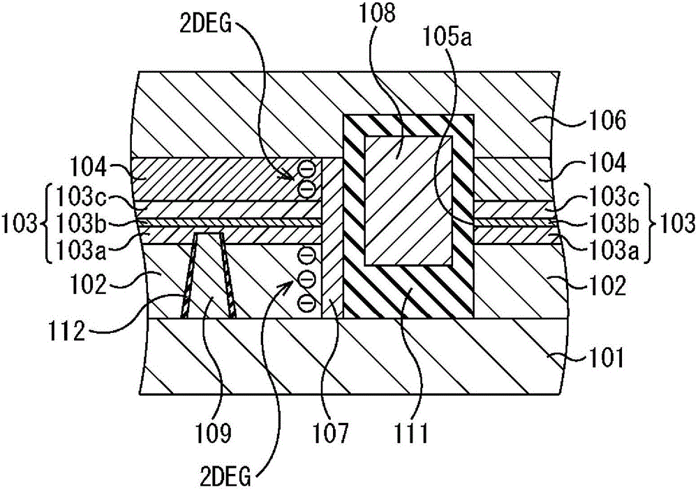
[0067] First, the first embodiment will be described. Figure 1A is a cross-sectional view showing the structure of the compound semiconductor device according to the first embodiment, Figure 1B It is a graph showing the energy of the conduction band in the first embodiment.

[0068] In the first embodiment, the compound semiconductor layer 102 , the compound semiconductor layer 103 , and the compound semiconductor layer 104 are sequentially formed on the drain electrode 101 . The laminated body 105 is constituted by the compound semiconductor layers 102 to 104 , and an opening 105 a is formed in the laminated body 105 . Furthermore, the compound semiconductor layer 107 in contact with the side surfaces of the compound semiconductor layers 102 to 104 is formed in the opening 105 a. A gate electrode 108 is also formed in the opening 105a. The gate electrode 108 is surrounded by an insulating film 111 . Therefore, the gate electrode 108 is insulated from the drain electrode ...

no. 2 Embodiment approach )

[0101] Next, a second embodiment will be described. Figure 2A is a diagram showing the positional relationship between electrodes of the compound semiconductor device according to the second embodiment, Figure 2B is along Figure 2A In the diagram of the section of the I-I line, Figure 2C is along Figure 2A A diagram of the cross-section of the line II-II.

[0102] In the second embodiment, a GaN layer 202, an AlGaN layer 203, GaN layers 204a and n are sequentially formed on a conductive substrate 221. + GaN layer 204b.

[0103] As the substrate 221 , for example, a conductive GaN single crystal substrate, a conductive sapphire substrate, a conductive SiC substrate, a conductive Si substrate, or the like can be used. In addition, in order to suppress the resistance component in the thickness direction of the board|substrate 221, it is preferable that the resistance of the board|substrate 221 is low. Examples of the conductive GaN single crystal substrate include a Ga...

no. 3 Embodiment approach )

[0153] Next, a third embodiment will be described. In the third embodiment, the source electrode 206 is formed before the gate electrode 208 . Figure 9A ~ Figure 9F It is a sectional view showing the manufacturing method of the compound semiconductor device of 3rd Embodiment in order of a process.

[0154] First, as in the second embodiment, the processes up to the formation of the AlGaN layer 207 are performed ( Figure 5A~Figure 5D ), and further, remove the silicon oxide film 252 ( Figure 7A ). Next, if Figure 9A shown, in n + The source electrode 206 is formed on the GaN layer 204 b and the AlGaN layer 207 . The source electrode 206 can be formed by, for example, a lift-off method.

[0155] Thereafter, if Figure 9B As shown, an insulating film 211a is formed on the source electrode 206 to planarize the surface. Furthermore, the insulating film 211a is processed by using the resist pattern 253 as a mask, and the electrode groove 226 is formed in the insulating f...


PUM


Abstract

An electrode (109) insulated from a compound semiconductor layer (102) and being in contact with an electrode (101) and a compound semiconductor layer (103) is provided. A lattice constant of the compound semiconductor layer (103) is smaller than both of a lattice constant of the compound semiconductor layer (102) and a lattice constant of a compound semiconductor layer (104), and a lattice constant of a compound semiconductor layer (107) is smaller than both of the lattice constants of the compound semiconductor layer (102) and the lattice constants of the compound semiconductor layer (107). A conduction band energy of the compound semiconductor layer (103) is higher than a conduction band energy of the compound semiconductor layer (104).

Description

technical field [0001] The present invention relates to a compound semiconductor device and a manufacturing method thereof. Background technique [0002] Conventionally, there has been a high electron mobility transistor (HEMT: high electron mobility transistor) in which an AlGaN layer and a GaN layer are formed by crystal growth on a substrate, and the GaN layer functions as an electron transport layer. GaN has a bandgap of 3.4eV, which is larger than that of Si (1.1eV) and GaAs (1.4eV). Therefore, GaN-based HEMTs have a high withstand voltage and are expected to be used as high-voltage power devices for automobiles and the like. [0003] On the other hand, a body diode must exist in a Si-based field effect transistor. The body diode is connected to the transistor in parallel in reverse, and functions as a freewheeling diode in a full-bridge circuit system that can be used in a high-power power supply. However, in a GaN-based HEMT, such a body diode does not necessarily ...

Claims


Application Information

Patent Timeline
Patent Type & Authority Patents(China)
IPC IPC(8): H01L21/338H01L21/336H01L21/8234H01L27/04H01L27/06H01L29/12H01L29/778H01L29/78H01L29/80H01L29/812H01L29/861
CPCH01L29/778H01L27/0605H01L29/0653H01L29/2003H01L29/205H01L29/66431H01L29/66462H01L29/7788H01L29/7789H01L29/41766H01L29/41741H01L29/045H01L27/0255H01L29/66219
Inventor 今田忠纮
Owner FUJITSU LTD
Why Eureka
Try Eureka