Glass spherical surface ultrasound focused cavitation reinforcement microreactor and preparation method thereof
A technology of ultrasonic focusing and microreactor, applied in the direction of chemical/physical/physicochemical processes of energy application, can solve repeatability and low reaction efficiency, energy waste, cavitation bubble appearance time, position uncertainty or randomness etc.
- Summary
- Abstract
- Description
- Claims
- Application Information
AI Technical Summary
Problems solved by technology
Method used
Image
Examples
Embodiment 1
[0035] A method for preparing a microfluidic grid on-chip experimental system integrating a spherical glass cavity focused ultrasonic transmitter, comprising the following steps:
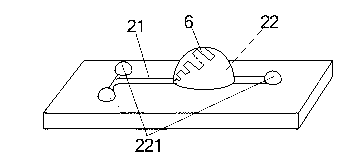
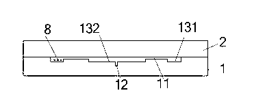
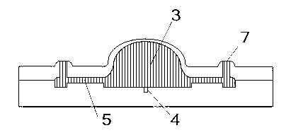
[0036] In the first step, a 5000 ? oxide layer is oxidized on a single-sided polished silicon wafer by a combination of dry and wet oxygen. The polished surface is spin-coated with AZ P4620 photoresist, exposed and developed to remove the photoresist that needs to be etched on the surface of the microcavity. Use Si micromachining technology to etch microchannel grooves and shallow grooves on a 4-inch Si wafer. The microchannel grooves connect the shallow grooves. The silicon wafer used can be a standard thickness silicon wafer with a thickness of 500 microns. The depth of the above-mentioned shallow grooves is 50-150 microns, the width of the small shallow grooves is 100-1000 microns, and the width of the large shallow grooves is 1000-10000 microns. Their shapes are square or circular, and the diamet...
Embodiment 2
[0046] A method for preparing a microfluidic grid on-chip experimental system integrating a spherical glass cavity focused ultrasonic transmitter, comprising the following steps:
[0047] In the first step, a 5000 ? oxide layer is oxidized on a single-sided polished silicon wafer by a combination of dry and wet oxygen, and the polished surface is spin-coated with AZ P4620 photoresist, exposed and developed to remove the photoresist that needs to be etched on the surface of the microcavity. Use Si micromachining technology to etch microchannel grooves and shallow grooves on a 4-inch Si wafer. The microchannel grooves connect the shallow grooves. The silicon wafer used can be a standard thickness silicon wafer with a thickness of 500 microns. The depth of the above-mentioned shallow grooves is 50-150 microns, the width of the small shallow grooves is 100-1000 microns, and the width of the large shallow grooves is 1000-10000 microns. Their shapes are square or circular, and the di...
PUM
| Property | Measurement | Unit |
|---|---|---|
| radius | aaaaa | aaaaa |
| thickness | aaaaa | aaaaa |
| depth | aaaaa | aaaaa |
Abstract
Description
Claims
Application Information


