Semiconductor etching device and etching method for semiconductor structure

An etching device and semiconductor technology, applied in the manufacture of semiconductor/solid-state devices, discharge tubes, electrical components, etc., can solve the problems of affecting the electrical properties of the semiconductor structure, affecting the bonding force, filling of the notch 1, etc., so as to improve the lithography accuracy and The effect of sidewall topography, avoiding systematic errors, and saving process costs

Active Publication Date: 2015-10-07
ADVANCED MICRO FAB EQUIP INC CHINA
View PDF1 Cites 0 Cited by
  • Summary
  • Abstract
  • Description
  • Claims
  • Application Information

AI Technical Summary

Problems solved by technology

[0004] But the inventor found that please refer to figure 1 , the through hole 2 formed by the method will have a notch 1 (notching) at the position in contact with the etch barrier layer 3, and the notch 1 is located between the semiconductor layer 4 and the etch barrier layer 3, which will affect the etching The binding force between the final semiconductor layer 4 and the etch stop layer 3, and when other materials are subsequently filled in the through hole 2, the incision 1 may not be completely filled, and voids will be formed in the formed semiconductor structure. , will affect the electrical properties of the semiconductor structure

Method used


Image

  • Semiconductor etching device and etching method for semiconductor structure
  • Semiconductor etching device and etching method for semiconductor structure
  • Semiconductor etching device and etching method for semiconductor structure

Examples


Embodiment Construction

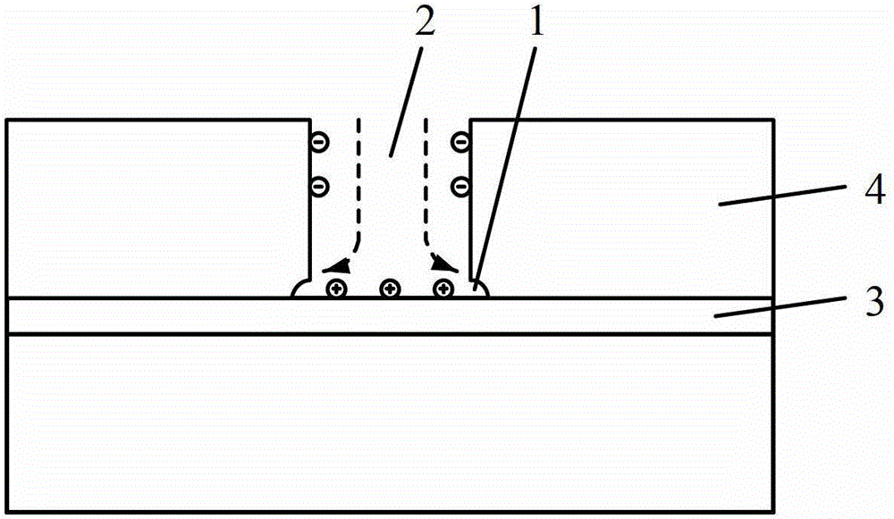
[0030] The inventors have found that in the existing multi-step etching process, the bias power source used to generate the bias voltage usually generates a continuous radio frequency signal, and uses the continuous radio frequency signal to generate continuous bias power, so that the to-be-etched The substrate surface has a bias voltage. When the plasma of the reactive gas reaches the surface of the substrate to be etched, please refer to figure 1 , due to the different angular distributions of positive ions and electrons in the plasma, positively charged positive ions tend to gather to the bottom of the structure to be etched, while negatively charged electrons tend to gather to the structure to be etched the top of. And because most of the existing etching barrier layers are insulating materials, when the surface of the etching barrier layer is etched, the positive ions gathered on the surface of the exposed etching barrier layer cannot be guided away, so that the positive...


PUM


Abstract

Disclosed are a semiconductor etching device and an etching method of a semiconductor structure. The etching method includes: a etching process with a first bias power source is utilized to etch a to-be-etched material layer, and the first bias power source generates continuous bias power to form a first opening which does not expose a etching blocking layer; and then a etching process with a second bias power source is utilized to etch the first opening, and the second bias power source generates pulse bias power until the etching blocking layer is exposed to form a second opening. Due to the fact that the continuous bias power is utilized to form bias voltage for etching firstly, side wall appearance is good, and etching selection ratio to a photo layer is high. The continuous bias power is switched into pulse bias power to form bias voltage for etching in prior to exposure of the etching blocking layer, so that cuts are avoided from being formed at the side wall bottom, close to the etching blocking layer, of the to-be-etched material layer.

Description

technical field [0001] The invention relates to semiconductor technology, in particular to a semiconductor etching device and an etching method for a semiconductor structure. Background technique [0002] In the semiconductor manufacturing process, it is usually necessary to etch the semiconductor layer to form deep via holes. In order to effectively control the depth of the deep via hole, it is necessary to form an etch stop layer before forming the semiconductor layer. Using the etch stop layer as an etch stop layer is conducive to the formation of a via hole with a precise depth. The etch stop layer is generally made of insulating materials such as silicon oxide and silicon nitride. Since the aspect ratio of etched via holes has reached 10:1, or even more than 30:1, in order to ensure the economic feasibility of the manufacturing process, these processes must be carried out at a relatively high etching rate to ensure reasonable production capacity , but at the same time...

Claims


Application Information

Patent Timeline
Patent Type & Authority Patents(China)
IPC IPC(8): H01L21/67H01J37/32H01L21/02H01L21/3065
Inventor 严利均仇松柏黄秋平许颂临
Owner ADVANCED MICRO FAB EQUIP INC CHINA
Why Eureka
Try Eureka