Array substrate, manufacturing method of array substrate, and display device
A technology of array substrates and substrates, applied in semiconductor/solid-state device manufacturing, optics, instruments, etc., can solve problems such as rising product costs and reduced production capacity of mass-produced products
- Summary
- Abstract
- Description
- Claims
- Application Information
AI Technical Summary
Problems solved by technology
Method used
Image

Examples
preparation example Construction
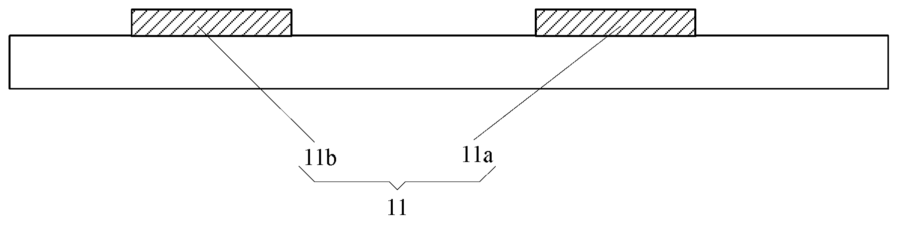
[0033] An embodiment of the present invention provides a method for preparing an array substrate, comprising: step 1, forming a patterned layer including a gate electrode on the substrate; step 2, forming a patterned layer including a gate insulating layer on the substrate that has completed the preceding steps; step 3. Form a patterned layer including an active layer on the substrate that has completed the preceding steps; Step 4. Form a transparent conductive film and a metal film sequentially on the substrate that has completed the foregoing steps, and form a pattern layer including the first electrode, data line, and source through a patterning process. The patterned layer of electrode, drain electrode and thin film field effect transistor (Thin Film Transistor, be called for short as TFT) channel; Step 5, form the patterned layer that comprises passivation layer on the substrate that finishes preceding steps; Step 6, finish preceding steps A pattern layer including the sec...
Embodiment 1
[0036] Embodiment 1, the preparation method of the array substrate, such as figure 1 shown, including the following steps:
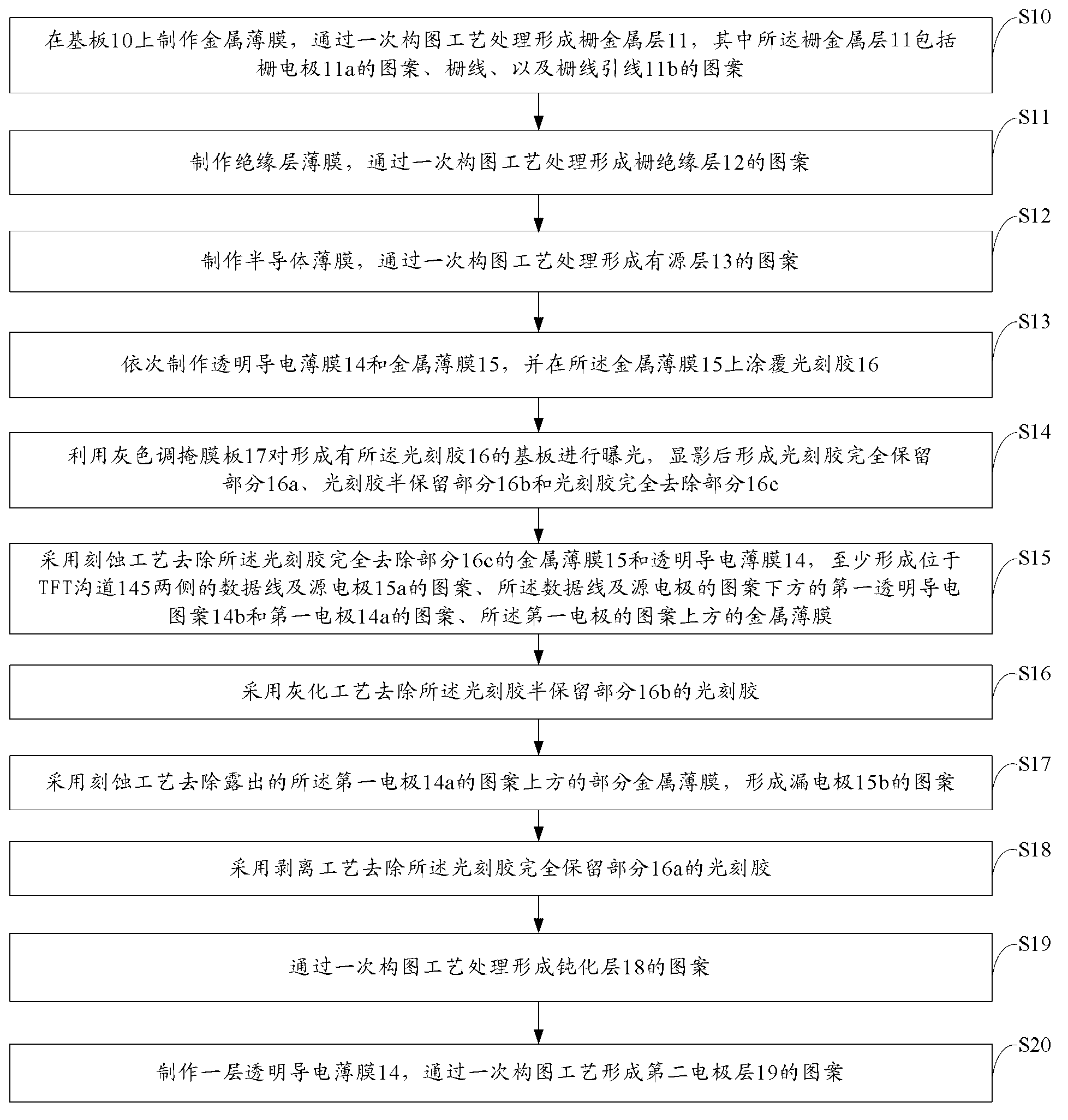
[0037] S10. Fabricate a metal thin film on the substrate, and form a patterning process such as figure 2 The gate metal layer 11 is shown, wherein the gate metal layer 11 includes a pattern layer of a gate electrode 11a, a gate line (not shown in the figure), and a pattern layer of a gate line lead 11b.
[0038] Specifically, a magnetron sputtering method can be used to prepare a layer with a thickness of to metal film. The metal material can usually be metals such as molybdenum, aluminum, aluminum-nickel alloy, molybdenum-tungsten alloy, chromium, or copper, or a combination structure of the above-mentioned thin films. Then, use a mask plate to process patterning processes such as exposure, development, etching, and stripping to form a pattern layer of gate electrodes 11a, gate lines (marked in the figure), and gate line leads 11b on a certain ar...
Embodiment 2
[0075] Embodiment 2, a method for preparing an array substrate, comprising the following steps:
[0076] S30, fabricate a metal thin film on the substrate, and form a gate metal layer 11 through a patterning process, wherein the gate metal layer 11 includes a pattern layer of a gate electrode 11a, a gate line (not shown in the figure), and a gate line lead 11b Make an insulating film on the substrate with the gate metal layer, and form a patterned layer of the gate insulating layer 12 with the first via hole 12a through a patterning process; on the substrate forming the patterned layer of the gate insulating layer 12 Make an active layer comprising one layer of amorphous silicon film and one layer of n+ amorphous silicon film, and form the pattern layer of active layer 13 comprising amorphous silicon pattern layer 13a and n+ amorphous silicon pattern layer 13b through a patterning process , formed as Figure 13 substrate shown.
[0077] Specifically, chemical vapor depositio...
PUM
 Abstract
Description
Claims
Application Information
 - R&D
- Intellectual Property
- Life Sciences
- Materials
- Tech Scout
- Unparalleled Data Quality
- Higher Quality Content
- 60% Fewer Hallucinations
Browse by: Latest US Patents, China's latest patents, Technical Efficacy Thesaurus, Application Domain, Technology Topic, Popular Technical Reports.
© 2025 PatSnap. All rights reserved.Legal|Privacy policy|Modern Slavery Act Transparency Statement|Sitemap|About US| Contact US: help@patsnap.com