Reverse conducting type insulated gate bipolar transistor without snapback effect

A bipolar transistor, reverse conduction technology, applied in the field of semiconductor power devices, can solve problems such as increasing the complexity of circuit design

Inactive Publication Date: 2013-04-03
UNIV OF ELECTRONICS SCI & TECH OF CHINA +1
View PDF2 Cites 33 Cited by
  • Summary
  • Abstract
  • Description
  • Claims
  • Application Information

AI Technical Summary

Problems solved by technology

[0006] Usually, an auxiliary circuit such as an RC snubber circuit can be added outside the device to improve the dynamic characteristics of the device and eliminate the snapback effect, but this will increase the complexity of the circuit design

Method used


Image

  • Reverse conducting type insulated gate bipolar transistor without snapback effect
  • Reverse conducting type insulated gate bipolar transistor without snapback effect
  • Reverse conducting type insulated gate bipolar transistor without snapback effect

Examples


Embodiment Construction

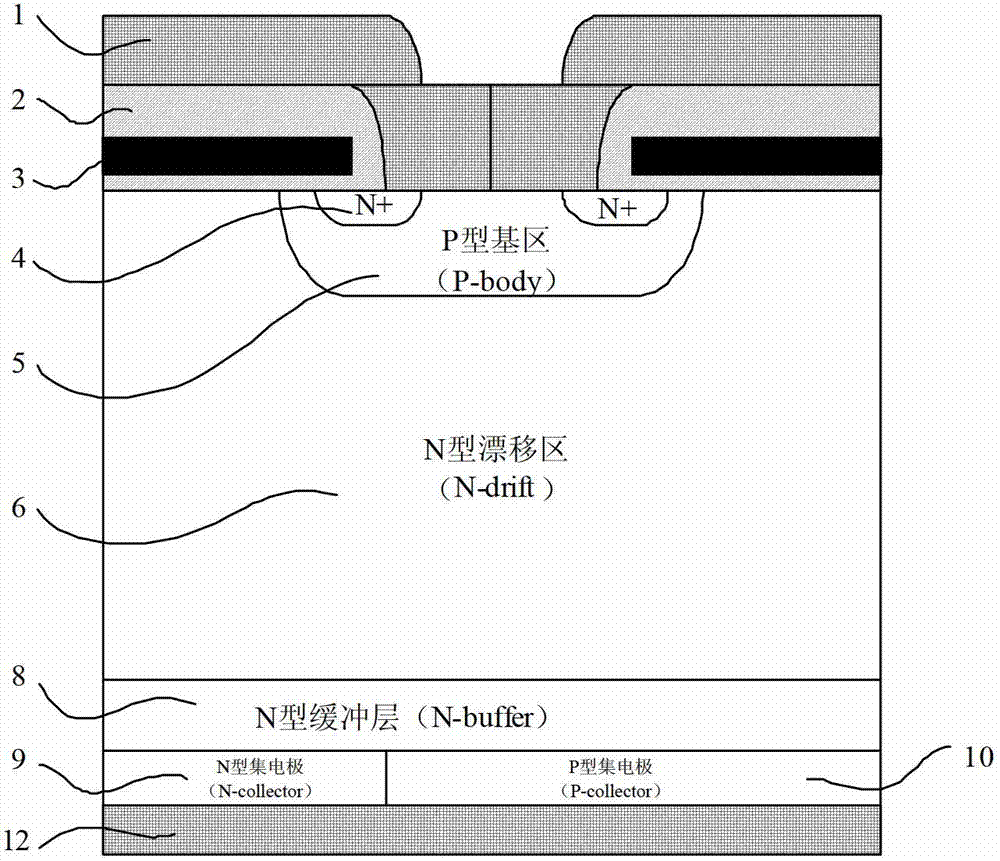
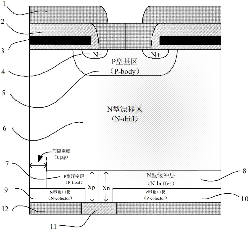
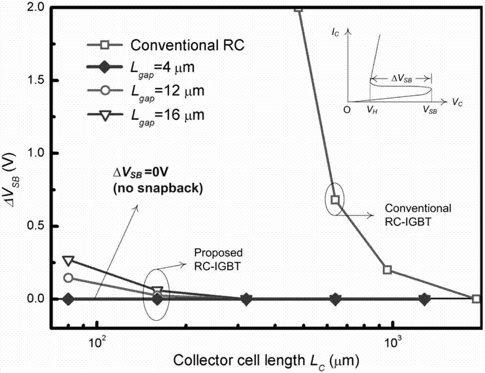
[0027] A reverse conducting insulated gate bipolar transistor without snapback effect, its structure is as follows figure 2 As shown, it includes metallized emitter 1, field oxide layer 2, polysilicon gate electrode 3, gate oxide layer, N+ source region 4, P body region 5, N- drift region 6, N buffer layer 8, N collector region 9 , P collector region 10 and metallized collector 12; P body region 5 is located on top of N-drift region 6, N+ source region 4 is located in P body region 5, and gate oxide layer is located in N+ source region 4, P body region 5 and The surface of the N-drift region 6, the polysilicon gate electrode 3 is located on the surface of the gate oxide layer, the metallized emitter 1 covers the remaining surfaces of the N+ source region 4 and the P body region 5, and the gap between the metallized emitter 1 and the polysilicon gate electrode 3 is Field oxide layer 2. The lower surface of the N-drift region 6 has a P floating region 7 and an N buffer layer 8...


PUM


Abstract

A reverse conducting type insulated gate bipolar transistor without a snapback effect belongs to the technical field of semiconductor power devices. A P floating region (7) is introduced between an N collector region (9) and an N buffer region (8) of a conventional RC-IGBT (Reverse Conducting-Insulated Gate Bipolar Transistor) so that the snapback effect of the reverse conducting type insulated gate bipolar transistor is eliminated, and the turn-off loss of the devices is reduced. The novel structure reduces the cellular length and the effective area of the N collector region (9) and increases the short-circuit resistance of a collector, the transmission efficiency of the P floating region (7) is higher than that of a P collector region (10), and the resistance of an N-drift region (6) is reduced through a conductance modulation effect, so that the snapback effect is eliminated. When the reverse conducting type insulated gate bipolar transistor reversely works, a parasitic transistor formed by the N-drift region (6), the P floating region (7) and the N collector region (9) is opened, so that a current path is provided, so as to form positive feedback of a PNPN (Positive-Negative-Positive-Negative) four-layer structure with the a P body region (5), the on-resistance when each device is reversely conducted is reduced, and the relatively low on-state voltage and the rapid shutdown are realized.

Description

technical field [0001] The invention belongs to the technical field of semiconductor power devices, and relates to an insulated gate bipolar transistor (IGBT). technical background [0002] With the continuous progress of science and technology and the rapid development of industry, the consumption of energy, especially electricity, is increasing day by day. How to save electricity and improve the efficiency of energy utilization has become an important topic today. In this context, semiconductor power devices represented by IGBTs came into being. [0003] IGBT (Insulated Gate Bipolar Transistor), insulated gate bipolar transistor, is a composite fully controlled voltage-driven power semiconductor device composed of BJT and MOS. IGBT not only has the advantages of fast working speed of MOSFET, high input impedance, simple driving circuit and good thermal temperature performance, but also has the advantages of large BJT current carrying capacity and high blocking voltage, wh...

Claims


Application Information

Patent Timeline
Patent Type & Authority Applications(China)
IPC IPC(8): H01L29/06H01L29/739
Inventor 陈万军蒋华平章晋汉张波
Owner UNIV OF ELECTRONICS SCI & TECH OF CHINA
Why Eureka
Try Eureka