Multi-quantum well layer growing method capable of improving LED luminance

A multi-quantum well layer and growth method technology, applied in the field of GaN material preparation, can solve problems such as limited effects, achieve good interception and storage effects, improve recombination efficiency, and reduce V-type defects

Active Publication Date: 2013-04-03
宁波安芯美半导体有限公司
View PDF4 Cites 32 Cited by
  • Summary
  • Abstract
  • Description
  • Claims
  • Application Information

AI Technical Summary

Problems solved by technology

The above method improves the radiative recombination efficiency

Method used


Image

  • Multi-quantum well layer growing method capable of improving LED luminance
  • Multi-quantum well layer growing method capable of improving LED luminance

Examples


Embodiment Construction

[0017] The embodiments of the present invention are described in detail below: the present embodiment is implemented under the premise of the technical solution of the present invention, and detailed implementation and specific operation process are provided, but the protection scope of the present invention is not limited to the following implementation example.

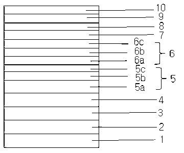
[0018] Such as figure 1 As shown, the LED epitaxial structure provided by the present invention includes: a substrate layer 1, a low-temperature GaN buffer layer 2, an undoped high-temperature GaN buffer layer 3, a Si-doped n-type GaN layer 4, a shallow quantum well 5, and multiple light-emitting layers. Quantum well 6, low-temperature p-type GaN layer 7, p-type AlGaN electron blocking layer 8, high-temperature p-type GaN layer 9, p-type GaN contact layer 10.

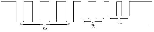
[0019] The multi-quantum well layer growth method for improving LED brightness provided by the present invention has specific implementation steps as follow...


PUM


Abstract

The invention relates to a multi-quantum well layer growing method capable of improving LED luminance. An LED epitaxial wafer structurally comprises a substrate layer, a low-temperature GaN buffer layer, an undoped high-temperature GaN buffer layer, a Si-doped n-type GaN layer, a light-emitting layer multi-quantum well, a low-temperature p-type GaN layer, a p-type AlGaN electron barrier layer, a high-temperature p-type GaN layer and a p-type GaN contact layer sequentially from bottom to top, the light-emitting layer multi-quantum well comprises a low-temperature shallow quantum well and a low-temperature multi-quantum well light-emitting layer sequentially from bottom to top, the low-temperature shallow quantum well comprises three shallow quantum well portions, well layers of the three shallow quantum well portions grow in a manner that indium content is gradually decreased, and barrier layers grow in a manner that content of TMAl (trimethylaluminum) fed to the barrier layers is gradually decreased. By the method, the LED luminance is improved by improving a shallow quantum well growth structure in the GaN-based LED quantum well.

Description

[0001] technical field [0002] The invention belongs to the technical field of preparation of GaN-based materials, and more specifically relates to a method for improving brightness by improving the growth structure of shallow quantum wells and the content of MO sources (metal organic sources) in GaN-based LED quantum wells. [0003] Background technique [0004] GaN (gallium nitride)-based materials are ionic crystals. Due to the misalignment of positive and negative charges, spontaneous polarization is formed; in addition, due to the lattice fit between InGaN (indium gallium nitride) and GaN materials, piezoelectric electrodes to form a piezoelectric polarization field. The existence of the polarization field, on the one hand, reduces the equivalent band gap of the quantum well and red-shifts the luminous wavelength; on the other hand, the overlap of the wave functions of electrons and holes decreases, reducing the probability of their radiative recombination. [000...

Claims


Application Information

Patent Timeline
IPC IPC(8): H01L33/00C30B29/40
Inventor 李永
Owner 宁波安芯美半导体有限公司
Why Eureka
Try Eureka